One chip, a dozen hands: the silicon side of the map
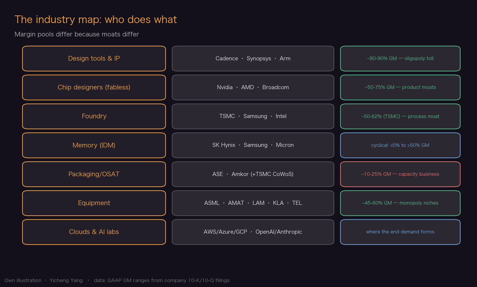
No company on Earth makes an AI chip alone. Think of publishing a book. Someone writes it, someone sells the word processor, someone licenses the fonts, a printing house prints it, machine makers built the presses, and a bindery assembles the final copies. The chip industry splits the same way, and each role has a name. EDA (electronic design automation) — Cadence, Synopsys, Siemens EDA — sells the design software: you cannot hand-draw 200 billion transistors, so every chip on the planet is designed inside these tools. IP vendors — Arm is the archetype — license pre-designed circuit blocks (a CPU core, a memory interface) and collect a royalty on every chip shipped. Fabless companies — Nvidia, AMD, Qualcomm, Broadcom — write the 'book': they design chips, build the software ecosystem, and own the customer, but operate no factories. Foundries — TSMC, Samsung Foundry, Intel Foundry — are the printing houses: contract manufacturers who turn designs into physical silicon; TSMC alone holds over 90% of the world's advanced-node capacity. IDMs (integrated device manufacturers) do both design and manufacturing in-house — Intel historically, and crucially the three memory makers (Samsung, SK Hynix, Micron), who mass-produce the HBM stacks every AI chip depends on. OSATs — ASE, Amkor — are the binderies: outsourced assembly, packaging, and test, historically the low-glamour end, though AI-era advanced packaging (Module 06's CoWoS) pulled the most valuable packaging work back into TSMC itself. Finally, equipment makers — ASML, Applied Materials, Lam Research, KLA, Tokyo Electron — build the presses: the lithography, deposition, etch, and inspection machines every fab must buy, with ASML holding a literal monopoly on EUV lithography.
From chip to token: the compute-economy layers
The map doesn't end when the chip is packaged — that's only where the AI-specific half begins. Hyperscalers — Microsoft, Google, Amazon, Meta — buy chips by the hundreds of thousands, build the datacenters, and sell the result as cloud computing. All four also design their own AI chips (Google's TPU, Amazon's Trainium, Microsoft's Maia, Meta's MTIA), which makes them part-time fabless companies and Nvidia's most dangerous customers. Neoclouds — CoreWeave, Nebius, and dozens of smaller firms — are specialist GPU landlords: they do one thing (rent out Nvidia GPUs by the hour) and their economics are pure real estate — borrow money, buy an asset, and earn a spread. An H100 costs a well-financed operator roughly $1.4–1.6 per GPU-hour all-in (capital, debt, power, datacenter) per SemiAnalysis TCO estimates, and rented for ~$2/hour at the best deals: a thin, leverage-sensitive margin, nothing like Nvidia's. AI labs — OpenAI, Anthropic, Google DeepMind, xAI — convert rented compute into models and sell tokens; they are the demand engine for everything upstream, and coding is the killer vertical — it drove Anthropic's API revenue up ~13x y/y, while OpenAI's mix still skews consumer chat (SemiAnalysis, Anthropic Growth and Bedrock Mix). A useful bridge metric across these layers: one megawatt of AI datacenter capacity generates roughly $10–12M of AI cloud revenue per year — which is why the industry increasingly quotes itself in megawatts and gigawatts rather than chips. When a lab signs a '1 GW deal,' you can now translate: about $10–12B a year of compute spending flowing up the chain you just mapped.
The margin ladder: why each layer earns what it earns
Line the layers up by gross margin — the share of each sales dollar left after direct production costs — and a striking ladder appears. EDA and IP sit at ~80–90%: software economics, a near-duopoly, and a price that is a rounding error next to the $100M+ chip project it enables. Nvidia earns ~75% on AI systems — it sells hardware at roughly 4x its build cost. TSMC printed 62.3% in 4Q25. Equipment makers cluster around 45–60% (KLA at the top). Memory swings wildly with the cycle — deeply negative in busts, above 50% in booms — because standard DRAM is a commodity; HBM is slowly making it less of one. OSATs scrape by at roughly 15–20%. The mechanism behind the ladder is not effort or even technology — it is scarcity times switching cost, divided by how visible your price is to the customer. EDA and ASML face almost no competition; Nvidia's CUDA software moat makes switching painful mid–AI race; TSMC's process lead means there is nowhere else to print a frontier chip. OSATs, by contrast, compete with each other on price for work anyone can do. One more axis matters: capital intensity. Nvidia's 75% needs no factories; TSMC's 62% must first pay for the most expensive factories ever built. High margin plus low capex (EDA, fabless) prints free cash flow; high margin plus brutal capex (TSMC, memory) is a treadmill where the margin is the reward for shouldering risk no one else will take.
Fab economics: the most expensive factories ever built
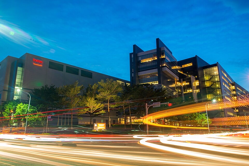
Foundry economics deserve their own stop on the map, because they gate everything else. The numbers are hard to absorb on first read. Intel says a leading-edge fab costs $25–30B of capex per 10,000 wafers per week of capacity; TSMC has cited about $42B per 10,000 wafers for its 3nm fabs in Arizona. TSMC's capital budget for 2026 alone is $52–56B — more than the annual capex of any Western oil major, and rivaling Saudi Aramco, the world's biggest oil spender (~$53B in 2024). A single EUV lithography tool costs ~$225M, and a fab needs dozens. Why does anyone sign up for this? Because each tool is a money press when busy: that $225M machine patterns more than $650M worth of wafers per year. The catch is the cost structure: a fab's costs are almost entirely fixed — depreciation (the giant purchase price expensed over ~5 years) plus staff and facilities that run 24/7 regardless of output. A fab resembles an airline: the marginal cost of filling one more seat (printing one more wafer) is small, and an empty slot is revenue lost forever. That makes utilization the single most important variable in foundry economics. In the 2023 downturn, TSMC's 7nm utilization fell from ~100% to below 60% within three quarters (≈83% in Q4'22 → <70% in Q1'23 → <60% in Q2'23), and margins sagged immediately. This is why foundries demand customer prepayments, why TSMC refuses to overbuild even when AI customers beg for wafers — underwriting a $40B fab against demand that might evaporate is how foundries die — and why the current AI boom keeps slamming into a silicon supply ceiling: capacity discipline learned in past busts.
Follow the AI capex dollar — and watch where the pool moves
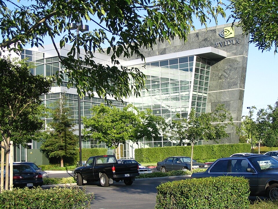
Now run one dollar of hyperscaler AI capex through the map. Most of it buys compute systems, and here the flow gets lopsided: Nvidia sells at ~75% gross margin, so of every dollar a cloud pays for an Nvidia system, roughly 75 cents stays in Santa Clara as gross profit and only ~25 cents flows on to the people who physically made it. Within the GPU chip's own build cost, HBM memory alone is about half — which is why the memory makers are the second-biggest AI winners — while TSMC's wafer and packaging take a smaller slice than most people guess. The markup applies to everything in the box: one GB200 rack carries ~$551k of optical transceivers at cost, which becomes ~$2.2M by the time the customer pays. The rest of the capex dollar buys networking, land, buildings, and increasingly power infrastructure. Then the dollar tries to come back: each megawatt deployed earns $10–12M a year of cloud revenue, out of which neoclouds keep a thin rental spread and labs keep whatever their token prices exceed compute costs. The key investing insight is that the pools move. In 2023–25 the money pooled at the bottlenecks: Nvidia, HBM, CoWoS packaging, then power equipment. By 2025–26, serving costs collapsed while token demand exploded, and value began pooling downstream in the model labs — Anthropic's inference gross margin swung from -94% in 2024 to 38% in 2025 to above 70% in 2026. The map is static; the money is not. Ask, every year: which layer is scarce now?


Key Numbers
| Metric | Value | Source |
|---|---|---|
| Nvidia gross margin on AI systems (≈4x markup over build cost) | ~75% | SemiAnalysis — GB200 Hardware Architecture - Component Supply Chain & BOM |
| Foundry capex intensity (TSMC, 2022 milestone) | $40-44B annual capex announced — far surpassing Intel and Samsung at the time | SemiAnalysis — TSMC Throws Down a $40B-$44B Gauntlet |
| Leading-edge fab capex intensity | Intel: $25–30B per 10k wafers/week; TSMC: ~$42B per 10k wafers at 3nm in Arizona | SemiAnalysis — Is Intel Back? Foundry & Product Resurgence Measured |
| HBM share of an H100-class AI chip's manufacturing cost | ~50% (nearly half) | SemiAnalysis — On Device AI – Double-Edged Sword |
| Taiwan's share of global advanced-node capacity (via TSMC) | >90% (and >60% of world foundry output) | SemiAnalysis — TSMC Overseas Fabs – A Success? |
| TSMC 7nm utilization swing in the 2023 downturn | ~100% → below 60% within three quarters (≈83% Q4'22 → <70% Q1'23 → <60% Q2'23) | SemiAnalysis — TSMC's Heroic Assumption – Low Utilization Rates, Fab Cancellation |
| AI cloud revenue per megawatt of datacenter capacity | $10–12M per MW per year | SemiAnalysis — How AI Labs Are Solving the Power Crisis: The Onsite Gas Deep Dive |
Sources
- SemiAnalysis — GB200 Hardware Architecture - Component Supply Chain & BOM
- SemiAnalysis — TSMC Throws Down a $40B-$44B Gauntlet
- SemiAnalysis — Is Intel Back? Foundry & Product Resurgence Measured
- SemiAnalysis — On Device AI – Double-Edged Sword
- SemiAnalysis — TSMC Overseas Fabs – A Success?
- SemiAnalysis — TSMC's Heroic Assumption – Low Utilization Rates, Fab Cancellation
- SemiAnalysis — How AI Labs Are Solving the Power Crisis: The Onsite Gas Deep Dive
- Wikimedia Commons — 曾成訓 (CC BY 2.0)
- Wikimedia Commons — Kevin McCarthy (CC BY 2.0)
- TSMC 4Q25 Earnings Release (Jan 15, 2026), pp.1–2 (verified via Wayback snapshot 20260117073643)
- SemiAnalysis — How To Kill 2 Monopolies With 1 Tool
- SemiAnalysis — Anthropic Growth and Bedrock Mix (with AI Value Capture — The Shift To Model Labs for the >70% 2026 figure)
- SemiAnalysis — The Great GPU Shortage: Rental Capacity
- SEC EDGAR XBRL — Amkor Technology GrossProfit
- SEC EDGAR XBRL — Synopsys GrossProfit
- SEC EDGAR XBRL — KLA Corp (Revenue less CostOfRevenue, 10-K)
- SEC EDGAR XBRL — Micron Technology GrossProfit
Related sector deep-dives
Optional — jump ahead if this module is all you needed; otherwise continue the ladder above.