Price the output, not the input: perf/TCO, MFU and $/Mtok
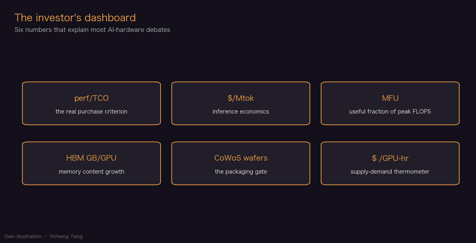
Most mistakes in AI hardware analysis start the same way: pricing an input (FLOPS, gigawatts, chips) instead of the output (useful tokens per dollar). Three metrics fix that.
TCO — total cost of ownership — is everything a GPU costs over its life: the chip, the servers, networking, power, cooling, and the downtime when it breaks. Perf per TCO divides realized throughput by that all-in cost, and it is the only ratio purchase decisions actually clear on. Example: a GB200 NVL72 rack costs ~1.6x an equivalent H100 fleet on TCO, so it must be ≥1.6x faster to deserve the order — whatever the keynote says.
MFU — model FLOPS utilization — is delivered math divided by the spec-sheet peak. Real training runs at 30-55%, and the number moves with zero hardware change: H100 BF16 MFU went 34%→54% in twelve months on CUDA software alone. So 'peak FLOPS' overstates reality by 2-3x, by a factor that itself keeps changing.
$/Mtok — dollars per million tokens — is where the whole chain cashes out. A GB300 NVL72 rack serving DeepSeek V4 gets to ~$0.156 per million output tokens; every layer of this series exists to push that figure down. And once power, not silicon, is the scarce input, perf/W becomes the tiebreaker: watts are fixed, so whoever converts them to tokens fastest wins the site.
Supply-side dials: HBM content, CoWoS, WFE, capex and cost per wafer
The supply chain publishes its own gauges, and each prices a different layer.
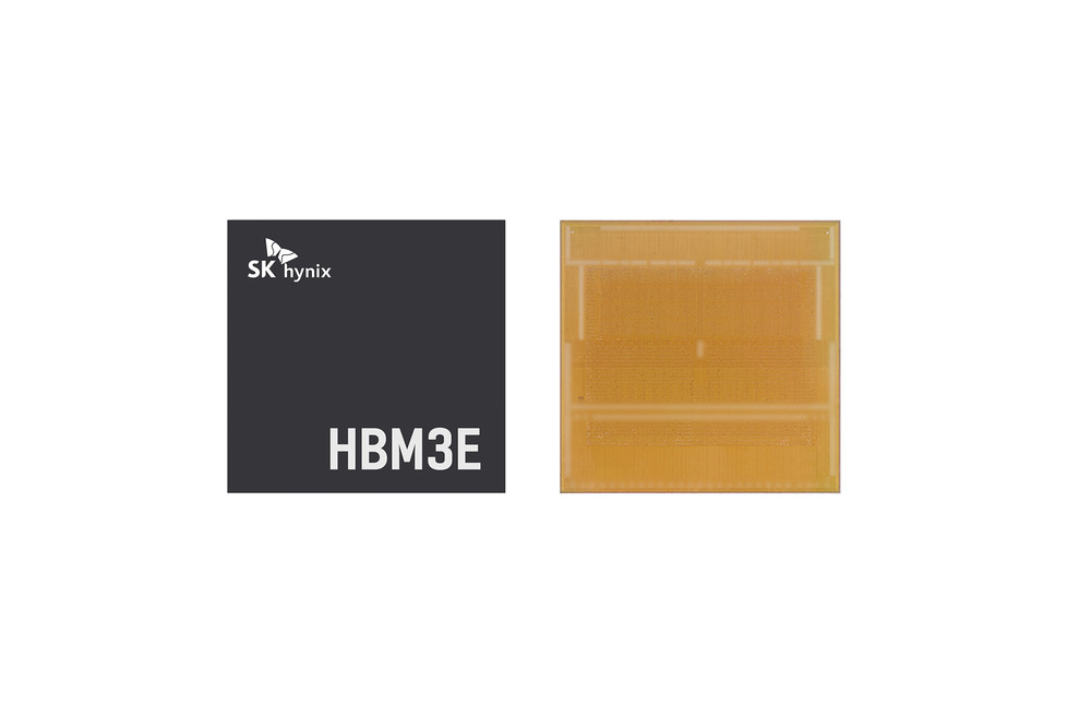
HBM content per GPU — how many gigabytes of stacked memory ride on each accelerator — is the memory sector's demand multiplier. HBM is already ~50%+ of an H100's manufacturing cost and ~60%+ on Blackwell: when Nvidia grows, SK Hynix's revenue line is mechanically dragged along.
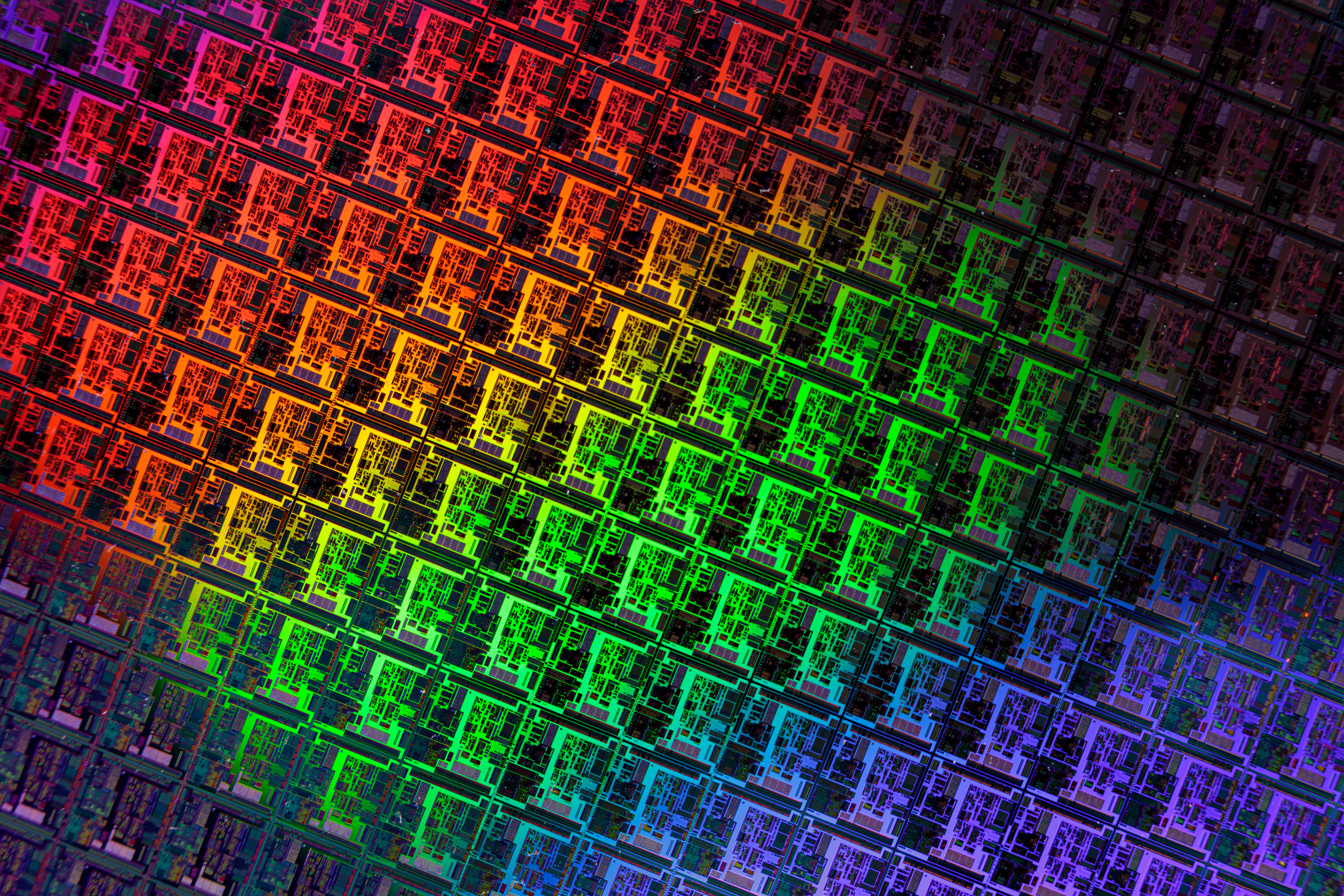
CoWoS capacity is the shipment forecaster. Every big AI GPU must pass through TSMC's advanced-packaging step, so its monthly wafer capacity — ~75,000 wafers/month in 2025, roughly double 2024 — caps unit shipments regardless of 'demand'. When someone forecasts GPU units, check the CoWoS arithmetic first.
WFE (wafer-fab equipment) spending is the tool layer's revenue pool, and capex intensity — capex over revenue — shows how hard a fab leans into the cycle: TSMC guided 2025 capex to $38-42B. That capex buys ever-pricier wafers (~$9,500 at N7 vs ~$16,000 at N5), while cost per transistor — the metric Moore's Law once improved automatically — gained only ~15% at N3, best case.
Finally, utilization (loadings): fabs are fixed-cost machines, so margins swing violently with how full they run. TSMC's N7 line went from 100% loaded to under 60% in the 2023 downturn — operating leverage in reverse.
Demand-side dials: rental $/GPU-hr, revenue per MW, RPO and goodput
If CoWoS is the supply gauge, the rental price of compute is the demand gauge. $/GPU-hr is the closest thing AI has to a spot price. Read it against cost: an H100 runs ~$1.53/hr all-in (including debt), so a $2.00+ rental prints healthy margin, and the price's direction is a real-time shortage signal — 1-year H100 rentals rose from $1.70 to $2.35/hr (+~40%) between October 2025 and March 2026, refuting the 'old chips must collapse' consensus.
Revenue per megawatt converts power into money: an AI cloud generates roughly $10-13M per MW per year, which is why 'speed to power' is a moat — energizing 200MW six months early carries an NPV of ~$400-500M.
RPO (remaining performance obligations) is contracted-but-unrecognized revenue on cloud balance sheets — the cleanest forward-demand series in public filings. Top GPU clouds booked ~$400B of it in roughly a year; when RPO growth stalls, believe it before the keynotes.
And inside the datacenter, goodput — the share of throughput that is useful work after crashes, stragglers and restarts — separates good clouds from cheap ones. A large pretrain can lose 6% of its budget to failures on a well-run cluster and 21% on a badly run one: a 15-point tax invisible in the hourly price.
Where the numbers live — and the four traps that eat analysts
Sources, in order of trustworthiness: (1) company IR — earnings calls, 10-K/6-K segment tables, capex guidance; TSMC even publishes monthly revenue. (2) Standards bodies (JEDEC) for what a spec actually guarantees, versus vendor overshoot. (3) Specialist trackers — TrendForce for memory pricing and CoWoS capacity, SemiAnalysis for delivered-performance benchmarks and TCO models. (4) keynotes and press releases — marketing until a number reappears in category 1.
Four traps. First, peak-FLOPS worship: spec sheets quote sparsity-doubled numbers almost no workload reaches, and cross-format comparisons flatter the newer chip — GB300 is '100x H100' only if H100 runs FP8 while GB300 runs FP4; same-format it is 65x. Always ask: which format, dense or sparse, what MFU?
Second, ignoring software maturity: MI355X throughput on DeepSeek V4 improved >100x in 26 days of kernel work. Day-0 benchmarks of new hardware are obituaries written before birth; the CUDA stack's compounding gains are a moat no spec sheet shows.
Third, announcement ≠ deployment: Microsoft walked away from >2GW of non-binding LOIs in 2025. Count binding contracts and RPO, not groundbreakings.
Fourth, know your index construction: a cap-weighted 'AI basket' is mostly Nvidia, TSMC and Broadcom — an incumbents bet — while an equal-weighted one quietly triples exposure to small, single-customer suppliers with far higher cycle beta. Same theme, different trade.
The glossary: the whole series in forty-three lines
One line each, in supply-chain order.
**Process node (N5/N3/N2/A16)** — marketing labels for transistor generations; the numbers measure nothing physical anymore. **Foundry / fabless / IDM** — who owns the fab: contract maker (TSMC), designer-only (Nvidia), or both-in-one (Intel). **Yield / D0** — share of dies that work; D0 is defects per cm², the number that decides it. **Tape-out / mask set** — freezing a design into photomasks; ~$40M per set at 3nm. **EUV / High-NA EUV** — ASML-monopoly lithography (~$225M/tool; High-NA ~$400M) printing the finest layers. **Multi-patterning** — splitting one fine layer across several cheaper exposures. **WFE** — wafer-fab equipment: the toolset (litho, etch, deposition, metrology) every fab must buy. **Utilization / loadings** — how full a fab runs; margins swing violently with it. **FinFET / GAA** — transistor architectures; GAA wraps the gate fully around the channel to keep scaling alive. **Backside power delivery** — power wiring moved beneath the transistors, freeing the top for signals. **Cost per transistor** — the metric Moore's Law used to improve automatically; now nearly stalled. **HBM / TSV** — DRAM dies stacked 8-16 high, wired by through-silicon vias; the memory that feeds GPUs at 3x+ DDR5 prices. **Stack-yield compounding** — per-layer yield multiplied across 12 layers; why HBM supply lags. **Memory wall** — compute outgrew memory bandwidth; most inference is bound by bytes, not FLOPS. **wspm** — wafer starts per month; the fab capacity unit. **Advanced packaging** — bump pitch below 100µm; chip-to-chip wiring as leading-edge tech. **CoWoS / interposer** — TSMC's 2.5D packaging seating GPU and HBM on a silicon carrier; gates AI GPU output. **Chiplet / KGD** — splitting one big die into tested smaller ones ('known good die') to beat defect math. **Hybrid bonding** — direct copper-to-copper stacking at micron pitches; the 3D endgame. **OSAT** — outsourced assembly-and-test firms (ASE, Amkor), the packaging tier below foundries. **SIMT / SM** — the GPU model: thousands of threads in lockstep across streaming multiprocessors. **Tensor Core / systolic array** — dedicated matrix engines amortizing instruction overhead into hundreds of ops. **Peak FLOPS** — the paper ceiling; often quoted 'with sparsity' at 2x what workloads reach. **FP8 / FP4** — low-precision formats; each halving doubles peak math if accuracy holds. **MFU** — model FLOPS utilization: delivered ÷ peak; 30-55% in real training. **Perf/W** — tokens per watt; the ranking that matters when power is the binding constraint. **TCO / perf-per-TCO** — all-in ownership cost, and the industry's true purchasing yardstick. **Scale-up vs scale-out** — the rack-level all-to-all fabric (NVLink, ~9x+ the cluster network, roughly an order of magnitude) vs the cluster network. **World size** — accelerators per scale-up domain (NVL72 = 72); decides which models serve cheaply. **Transceiver / DSP** — pluggable optics; the biggest cost and power line in cluster networking. **CPO** — co-packaged optics: optics moved onto the switch package, deleting the DSP and ~2/3 of link power. **OCS** — optical circuit switching with mirrors (~108W vs ~3,000W electronic); Google's pod glue. **PUE / WUE** — facility power (or water) ÷ IT power; hyperscalers ~1.1 vs industry ~1.6. **BTM** — behind-the-meter: building your own generation instead of queueing years for grid power. **$/GPU-hr / neocloud** — compute's spot price, and the GPU-only clouds (CoreWeave) that set it. **RPO** — contracted-but-unrecognized revenue; the cleanest forward-demand gauge in filings. **Goodput** — useful work as a share of raw throughput, after failures and restarts. **$/Mtok** — dollars per million tokens; the end-product unit cost the whole chain works to cut. **Prefill vs decode** — inference's two phases: compute-bound prompt reading vs bandwidth-bound token writing. **KV cache** — stored attention state growing with context length; long-context memory hog. **MoE** — mixture-of-experts: only a slice of the model computes per token, trading FLOPS for memory and interconnect. **FDPR / Entity List** — US export-control levers: reach foreign-made goods via US tech content; blacklist named firms. **Die bank** — stockpiled dies (Huawei banked 2.9M+ from TSMC) that keep a sanctioned firm shipping for years.

Key Numbers
| Metric | Value | Source |
|---|---|---|
| GB200 NVL72 total cost of ownership vs an equivalent H100 fleet | ~1.6x — so it must be ≥1.6x faster to win on perf-per-TCO | SemiAnalysis — H100 vs GB200 NVL72 Training Benchmarks - Power, TCO, and Reliability Analysis |
| H100 training MFU gain from software alone (12 months, no hardware change) | BF16 MFU 34% → 54% (+~59% throughput) | SemiAnalysis — H100 vs GB200 NVL72 Training Benchmarks - Power, TCO, and Reliability Analysis, Software Improvement Over Time |
| State-of-the-art serving cost, GB300 NVL72 running DeepSeek V4 | $0.156 per 1M output tokens (50 tok/s/user, 8k in / 1k out) | SemiAnalysis — DeepSeekV4 1.6T Day 0 to Day 43 Performance Over Time - Huawei, GB300 NVL72, MI355X, B200 |
| HBM share of AI GPU manufacturing cost | H100 ~50%+ → Blackwell ~60%+ | SemiAnalysis — The Memory Wall: Past, Present, and Future of DRAM |
| 1-year H100 rental price move, Oct 2025 → Mar 2026 | $1.70 → $2.35 per GPU-hour (+~40%); all SKUs sold out on-demand | SemiAnalysis — The Great GPU Shortage – Rental Capacity |
| TSMC 2025 capital budget (official guidance) | US$38-42 billion | TSMC — Fourth Quarter 2024 earnings press release |
| TSMC CoWoS advanced-packaging capacity, 2025 | ~75,000 wafers/month — nearly double 2024 levels | TrendForce — TSMC Set to Expand CoWoS Capacity to Record 75,000 Wafers in 2025 |
Sources
- SemiAnalysis — H100 vs GB200 NVL72 Training Benchmarks - Power, TCO, and Reliability Analysis
- SemiAnalysis — DeepSeekV4 1.6T Day 0 to Day 43 Performance Over Time - Huawei, GB300 NVL72, MI355X, B200
- SemiAnalysis — The Memory Wall: Past, Present, and Future of DRAM
- SemiAnalysis — The Great GPU Shortage – Rental Capacity
- TSMC — Fourth Quarter 2024 earnings press release
- TrendForce — TSMC Set to Expand CoWoS Capacity to Record 75,000 Wafers in 2025
- Wikimedia Commons (CC BY 2.0, photo by Rob Bulmahn)
- SK hynix Newsroom
- SemiAnalysis — Advanced Packaging Part 1 (N7 ~$9,500 vs N5 ~$16,000 per wafer)
- SemiAnalysis — TSMC's 3nm Conundrum (N3 ~15% cost-per-transistor improvement, weakest scaling)
- SemiAnalysis — TSMC's Heroic Assumptions & Low Utilization (N7 loadings fell below 60% in the 2023 downturn)
- SemiAnalysis — GPU Cloud Economics Explained (H100 all-in ~$1.525/hr with 13% debt; best deals ~$2/hr)
- SemiAnalysis — To Boldly Go: The Case for Space Datacenters (~$12-13M revenue/MW; 200MW six months early = ~$400-500M NPV)
- SemiAnalysis — How AI Labs Are Solving the Power Problem (AI cloud revenue ~$10-12M per MW annually)
- SemiAnalysis — ClusterMax 2.0 (top neoclouds have booked nearly $400Bn of RPO)
- SemiAnalysis — InferenceX v2: Nvidia Blackwell (GB300 100x on FP8-vs-FP4 vs H100; 65x same-format FP8)
- SemiAnalysis — Microsoft's Datacenter Freeze (walked away from >2GW of non-binding LOIs)
- SemiAnalysis — How To Kill 2 Monopolies With 1 Tool (EUV ~$225M/tool; High-NA EXE:5000 ~$400M)
- SemiAnalysis — Datacenter Anatomy Part 1: Electrical (NVLink scale-up ~9x inference throughput)
- SemiAnalysis — Google Apollo: The $3 Billion Game (OCS uses ~108W vs ~3,000W for a 136-port electronic switch)
- SemiAnalysis — Datacenter Anatomy Part 2: Cooling (Google/Meta ~1.1 PUE, MSFT/AWS ~1.15 vs enterprise colo ~1.5-1.6)
- SemiAnalysis — Huawei Ascend Production Ramp (Huawei received >2.9M Ascend die from TSMC)
Related sector deep-dives
Optional — jump ahead if this module is all you needed; otherwise continue the ladder above.