Why packaging hit the front page
For fifty years, 'more computing' had a single recipe: shrink the transistor. Packaging — the final step that wraps a finished die in a protective shell and connects it to the circuit board — was an afterthought, outsourced to low-margin assembly houses. Around 2020 that quietly inverted, because three walls closed in at once.
First, the reticle limit. A lithography scanner projects a chip design through a photomask onto the wafer one exposure at a time, and the largest field it can expose is 26mm × 33mm — about 858mm². You physically cannot print a bigger single chip. Nvidia's datacenter GPUs have been pressed against this ceiling for years; 'just make it bigger' is no longer an option.
Second, yield. Defects scatter across a wafer roughly at random, like darts at a board. Double a die's area and you roughly double its odds of catching a killer defect, so the cost of a good chip rises much faster than its size. The biggest chips are exactly the ones you can least afford to build.
Third, and least appreciated: IO stopped scaling. Transistor density doubled about every two years, but chip-to-package data rates doubled only every four — and the solder bumps that carry signals off the die barely shrank from 2000 to 2021 (from ~200µm down to only ~100-130µm — a 2× shrink while transistor density rose ~1,000×). Many designs became 'pad-limited': die area set by connection pads, not by logic. Add that wafer prices jumped from ~$9,500 (N7) to ~$16,000 (N5), ending the free fall in cost-per-transistor, and the industry's only remaining lever is how dies get wired together. That lever is advanced packaging.
Chiplets: bargaining with defect math
The first response is to stop building monoliths. Split one huge die into several small 'chiplets' and the defect lottery changes in your favor: a dart that lands on a small die scraps a cheap fragment, not an $800 flagship. Just as important, each piece can be tested before assembly, so you only combine Known Good Die (KGD) — a three-letter idea that quietly governs almost every packaging decision in this module. AMD ships everything from 8-core desktops to 64-core servers by reusing one small compute chiplet, covering with 3 chip designs a market Intel needed 5 monolithic designs to span — and it mixes process nodes, putting compute on the newest node and IO on an older, cheaper one.
But chiplets are a tool, not a religion. Every split adds interface circuits that burn area and power, plus a packaging step that can itself fail. SemiAnalysis's cost model exposes a subtler tax: lithography is roughly a third of wafer cost, and the scanner exposes fixed 26×33mm fields — a chiplet that tiles that field badly needs 1.875× the exposures, repricing the wafer from $17,000 to $21,364 and shrinking the chiplet's silicon saving from $136 to $26 per part, before packaging costs are even counted. Intel's Emerald Rapids server chip actually re-aggregated four chiplets back into two large dies. Whether to split depends on yield, reticle geometry and interface overhead — and the answer can flip either way.
2.5D and CoWoS: a silicon table for GPU and HBM
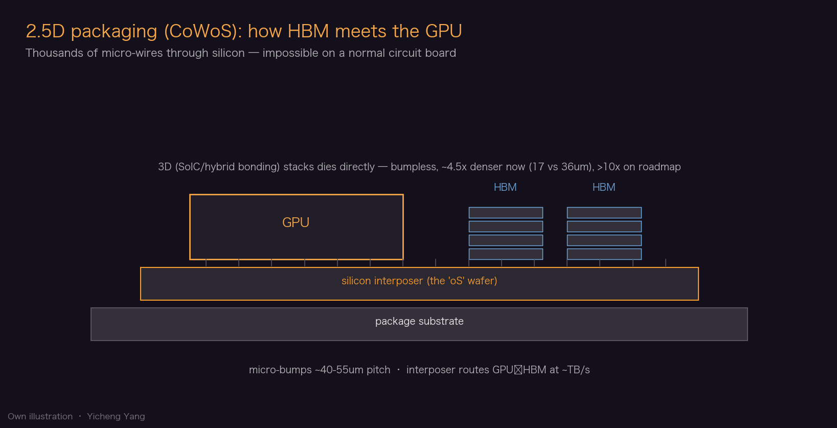
AI made one wiring problem urgent: a GPU must talk to its memory over an extremely wide, extremely short bus. High Bandwidth Memory (HBM) gets its bandwidth from width, not clock speed — each stack connects through over a thousand data wires (HBM4 doubles that again). No ordinary package substrate or circuit board can route a thousand traces per stack; the wires would be too coarse and too long.
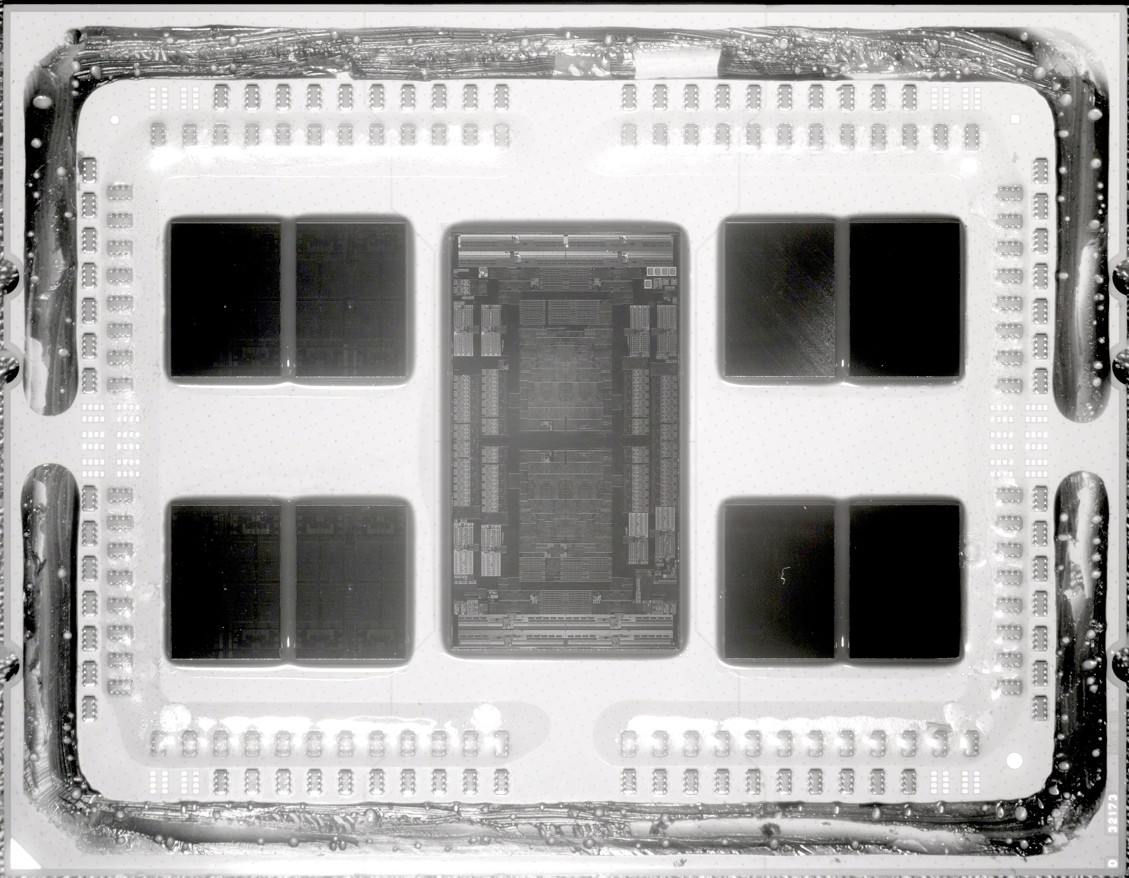
The 2.5D answer: lay the compute die and the HBM stacks side by side on top of another piece of silicon. Because that base slab is patterned with chip lithography, its wires can be one to two orders of magnitude finer (~25× vs a modern ABF substrate). The slab — the 'interposer' — does no computing; it is pure wiring, plus TSVs (through-silicon vias): vertical copper shafts that pass power and signals up from the package below. TSMC's brand for this sandwich is CoWoS — Chip-on-Wafer-on-Substrate. Essentially every Nvidia and AMD AI accelerator is compute dies plus HBM sitting on some flavor of it.
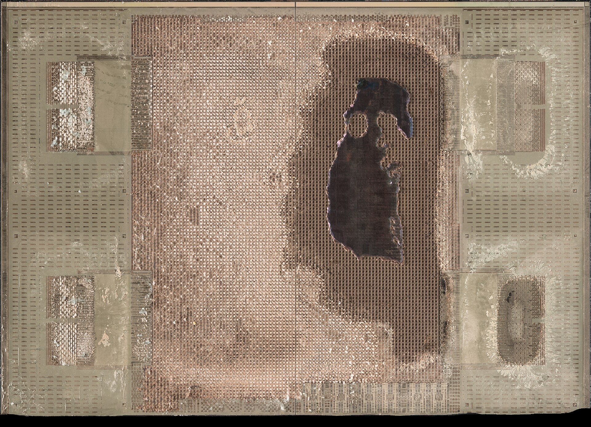
Interposers are expensive: TSV formation is slow, tool-hungry and, per SemiAnalysis, a genuine bottleneck for both CoWoS and HBM output. Hence the variants. CoWoS-R swaps silicon for cheaper organic RDL wiring; bridge approaches — Intel's EMIB, TSMC's CoWoS-L — embed only a small sliver of silicon where two die edges actually meet. And as AI packages outgrow the reticle itself, interposers are 'stitched' together from multiple exposures: the interposer under a 2016 Tesla P100 was already ~1,166mm², larger than any chip that can be printed in one shot.
3D: micro-bumps vs bumpless hybrid bonding
2.5D still spreads dies sideways; the tightest connection is to stack them vertically, dropping interconnect distances from millimeters to microns and collapsing the energy each bit costs to move.
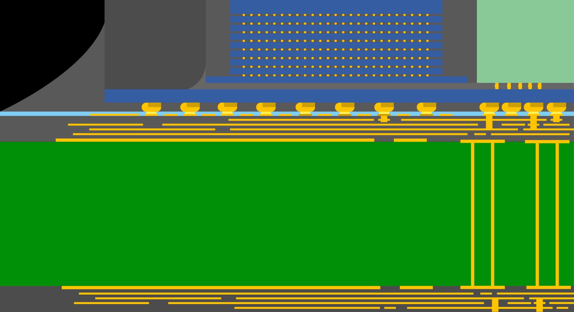
Generation one is micro-bump 3D: the same solder-ball idea, miniaturized to ~36µm pitch — 31× the connection density of standard flip chip. But solder has a floor: much below ~20µm pitch the bumps short into each other, and every joint adds resistance.
Hybrid bonding removes solder entirely. Both surfaces are polished to sub-nanometer flatness; the dielectric faces bond on contact, and copper pads recessed ~5 nanometers below the surface expand during a bake until they fuse — copper to copper, 'bumpless'. Pitches drop below 10µm with a roadmap into the hundreds of nanometers. AMD's 3D V-Cache, the first mass-market logic product, runs a 17µm pitch — ~138× flip-chip density. SemiAnalysis calls hybrid bonding the most transformative manufacturing innovation since EUV.
It comes with brutal physics. A particle just 1µm tall creates a bond void ~10mm across — one speck of dust kills a fingernail-sized patch of connections. That demands ISO 1-3 cleanrooms and front-end fab tools (deposition, electroplating, precision CMP polishing) that traditional packaging houses — OSATs like ASE and Amkor — simply don't own. This is the structural punchline: hybrid bonding moved leading-edge packaging inside the fab (TSMC's SoIC, Intel's Foveros Direct), turning 'assembly' from cheap outsourced labor into foundry business. One trade-off to remember: wafer-on-wafer bonding aligns whole wafers to under 50nm but cannot screen out bad dies, while die-to-wafer places only Known Good Die but is slower and dirtier.
The family album: InFO, EMIB, Foveros
Three names you will meet constantly — one paragraph each.
InFO (TSMC, 'Integrated Fan-Out') solves a different problem: a die that needs more connections than its own footprint can hold. The die is embedded in molding compound and its IO is 'fanned out' across that larger artificial surface through fine RDL wiring — no substrate needed, thinner and cheaper than 2.5D. Every iPhone processor since 2016's A10 ships in InFO, and the wafer-scale variant, InFO_SoW, packaged the 25-die training tile of Tesla's Dojo supercomputer.
EMIB (Intel, 'Embedded Multi-die Interconnect Bridge') is the anti-interposer: instead of a full slab of silicon under everything, embed a fingernail-sized silicon bridge into the organic substrate exactly under the seam where two dies meet. You get interposer-class wiring density where the traffic actually flows, and cheap substrate everywhere else. Intel's Sapphire Rapids Xeons mix 55µm-pitch EMIB regions with 100µm standard bumps on a single package.
Foveros (Intel) is the 3D entry: true die-on-die stacking on ~36µm micro-bumps — Meteor Lake stacks its compute tile on a base tile — with Foveros Direct as the bumpless, hybrid-bonded successor. A mental map for everything above: CoWoS and EMIB place dies side-by-side (2.5D); Foveros and SoIC stack them vertically (3D); InFO spreads one die's connections outward (fan-out).
The new bottleneck — and the new profit pool
Since 2023, whenever Nvidia GPUs were scarce, the binding constraint was usually not wafers — TSMC could print the compute dies — but CoWoS capacity and HBM supply. 'Advanced packaging' became, in effect, the production schedule of AI compute.
The money followed. TSMC's CoWoS revenue grew from about $0.6B in 2018 to $9.6B in 2025 — 2.5× what Apple's InFO brings in — and advanced packaging passed 10% of TSMC's total revenue. A step once priced in cents per chip now prices in hundreds of dollars per AI accelerator.
Inside the flow, the chokepoints are specific and investable. TSV formation — the etch-and-plate sequence that drills the vertical vias — bottlenecks both HBM and CoWoS. HBM's stacking arithmetic compounds the problem: 12-high stacks force each DRAM die to be thinned to 30µm — SK Hynix bonds all layers at once with MR-MUF (mass reflow), while Samsung and Micron use slower thermocompression (TC-NCF/TCB). And hybrid-bonding die placers trade throughput against accuracy so brutally that rated speeds roughly halve in practice.
Because hybrid bonding is a front-end process, each new generation shifts value away from OSATs toward foundries and fab-tool vendors — deposition, CMP, dicing, bonders. So when a headline says 'TSMC doubles CoWoS capacity', read it as: that is the ceiling on next year's AI accelerator shipments — and the toll for that ceiling accrues to a shrinking list of companies.



Key Numbers
| Metric | Value | Source |
|---|---|---|
| Reticle limit (largest printable die) | 26mm × 33mm ≈ 858mm² per exposure field | SemiAnalysis — Die Size And Reticle Conundrum – Cost Model With Lithography Scanner Throughput |
| Transistor vs IO scaling | Transistor density 2× every ~2 years; chip IO data rates 2× every ~4 years | SemiAnalysis — Advanced Packaging Part 1 – Pad Limited Designs |
| Interconnect density ladder (vs standard 150-200µm flip chip) | Fanout ~8× → 2.5D interposer ~16× → 36µm micro-bump 3D 31× → 17µm hybrid bonding (V-Cache) 138× → Sony 6.3µm CIS 567× (the 150-200µm standard flip-chip baseline is not uniform across rungs) | SemiAnalysis — Advanced Packaging Part 1 – Pad Limited Designs |
| Wafer price, N7 vs N5 | ~$9,500 (N7) vs ~$16,000 (N5) — cost-per-transistor stopped falling | SemiAnalysis — Advanced Packaging Part 1 – Pad Limited Designs |
| TSMC CoWoS revenue, 2025 | $9.6B — 2.5× InFO, up from ~$0.6B in 2018 | SemiAnalysis — Apple-TSMC: The Partnership That Built Modern Semiconductors |
| Hybrid bonding particle sensitivity | A particle just 1µm tall → a bond void ~10mm in diameter | SemiAnalysis — Hybrid Bonding Process Flow - Advanced Packaging Part 5 |
| HBM die thinning (SK Hynix 12-hi HBM3) | Each DRAM die thinned to 30µm — SK Hynix bonds 12-hi via MR-MUF (mass reflow); Samsung/Micron use slower thermocompression (TC-NCF/TCB) | SemiAnalysis — Advanced Packaging Part 3 – Intel's Curious Bet on Thermocompression Bonding |
Sources
- SemiAnalysis — Die Size And Reticle Conundrum – Cost Model With Lithography Scanner Throughput
- SemiAnalysis — Advanced Packaging Part 1 – Pad Limited Designs
- SemiAnalysis — Apple-TSMC: The Partnership That Built Modern Semiconductors
- SemiAnalysis — Hybrid Bonding Process Flow - Advanced Packaging Part 5
- SemiAnalysis — Advanced Packaging Part 3 – Intel's Curious Bet on Thermocompression Bonding
- Wikimedia Commons — Fritzchens Fritz (CC0)
- Wikimedia Commons — 思考的苇丛 (CC BY-SA 4.0)
- Wikimedia Commons — Fritzchens Fritz (CC0)
- Fritzchens Fritz — Flickr die-shot measurement (Interposer = ~1,165.65mm², 40,167 × 29,020 µm)
- Wikipedia — High Bandwidth Memory
- Wikipedia — Apple A10 ('The A10 is packaged in a new InFO packaging from TSMC')
- SemiAnalysis — Intel Emerald Rapids Backtracks on Chiplets
- SemiAnalysis — IEDM 2022 Part 1 (EMIB 55µm in Sapphire Rapids) + Advanced Packaging Part 1 (Intel 10nm 100µm flip chip)
- SemiAnalysis — Packaging Developments From ECTC 2022
- SemiAnalysis — Tesla Dojo: Unique Packaging and Chip Design
- SemiAnalysis — AI Capacity Constraints: CoWoS and HBM Supply Chain
- SemiAnalysis — Advanced Packaging Part 2: Review of Options
Related sector deep-dives
Optional — jump ahead if this module is all you needed; otherwise continue the ladder above.