Why computers need a memory pyramid
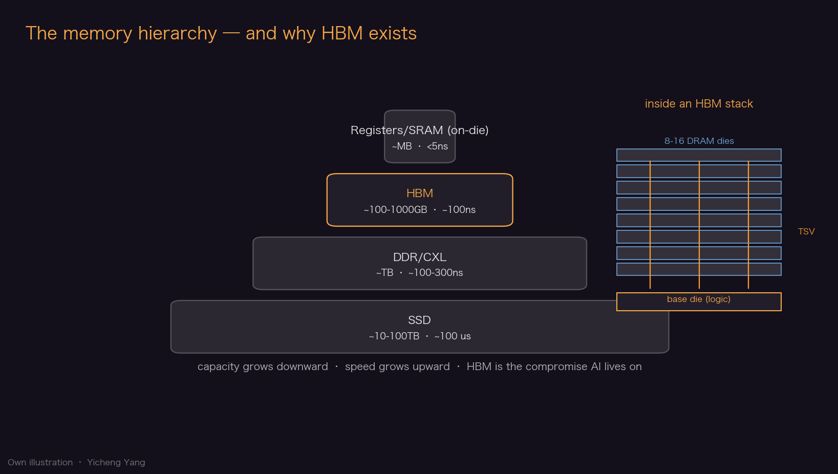
A processor can only compute on data it is holding right now. The trouble is that memory fast enough to keep up with a processor is astronomically expensive per bit, and memory cheap enough to buy in bulk is painfully slow. Engineers resolve this with a hierarchy — a pyramid of layers, each one bigger, cheaper, and slower than the one above it.
At the tip sit registers: a few kilobytes inside the CPU or GPU core itself, reachable in under a nanosecond — the pages you are literally holding in your hands. Next comes SRAM cache (tens of megabytes, roughly 1-30 nanoseconds) — the desk in front of you. SRAM is fast because every bit is an actively powered six-transistor circuit; but that is exactly why it stays small, costing roughly 20x more silicon area per bit than DRAM. Below that lies main memory built from DRAM: tens to hundreds of gigabytes at roughly 100 nanoseconds — the bookshelf across the room. At the base, NAND-flash SSDs hold terabytes at around 100 microseconds — a warehouse across town: a thousand times slower again, but nearly free per bit.
The pyramid works because programs normally reuse the same data over and over ('locality'). AI broke that comfort. A trillion-parameter model fits in no cache, and inference streams essentially the whole model through the chip for every single token it generates. AI needed a new layer wedged between SRAM and ordinary DRAM — DRAM re-packaged for extreme bandwidth. That layer is HBM.
One transistor, one capacitor — and why DRAM stopped shrinking
DRAM's beauty is its brutal simplicity. Each bit is one transistor plus one capacitor — the '1T1C' cell. The capacitor stores electric charge (charged means 1, empty means 0); the transistor is the gate that reads or writes it. Because capacitors leak, every cell must be refreshed every few tens of milliseconds — dozens of times per second — that is the 'dynamic' in Dynamic RAM. This one-transistor design is why DRAM is ~20x denser than SRAM and cheap enough to buy by the gigabyte.
The same capacitor is what killed DRAM scaling. To produce a signal the sense amplifier can still detect, a cell must trap on the order of 40,000 electrons. Shrink the cell's footprint and the capacitor can only keep its surface area by growing taller — modern DRAM capacitors are wells with roughly 100:1 aspect ratios, skyscrapers in silicon. In the golden age, DRAM density doubled every 18 months, about 100x per decade. Over the last decade it managed roughly 2x. As SemiAnalysis puts it, Moore's Law for DRAM died over a decade ago — with zero fanfare.
The investment consequence is enormous. With no cost-down left to cushion prices, DRAM behaves like a commodity with almost perfectly inelastic supply: the only way to add bits is to build new fabs, which takes years. That is the structural reason the industry consolidated into three players controlling over 95% of supply — SK Hynix, Samsung, Micron — and why the memory cycle swings so violently.
HBM: when you can't shrink, stack
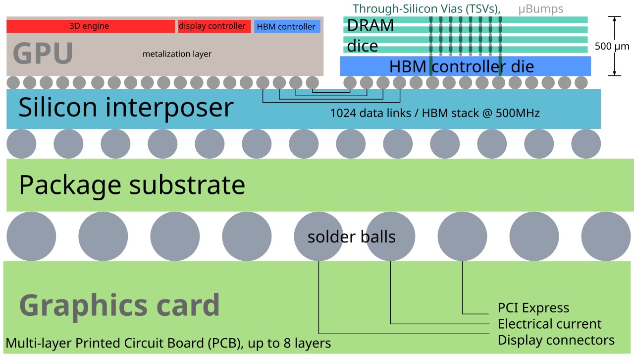
HBM (High Bandwidth Memory) does not fix DRAM's physics; it re-packages them. Take 8 to 16 DRAM dies, grind each down to a fraction of a hair's thickness, drill thousands of vertical copper channels straight through them — through-silicon vias (TSVs), the elevator shafts of the stack — and mount the tower on a base die that manages traffic in and out. The result is a cube of memory.
The real trick is the bus. An ordinary DDR module talks to the CPU over roughly 64 data wires driven very fast across centimeters of circuit board. HBM inverts the design: 1,024 wires (2,048 in HBM4), each running at a moderate speed, over just a few millimeters. Wide-and-slow beats narrow-and-fast on both total bandwidth and energy per bit. But a thousand-plus wires cannot be routed through a printed circuit board — its traces are far too coarse. So the cube must sit right next to the GPU on a silicon interposer, a slice of silicon whose wiring is fine enough, joined by TSMC's CoWoS packaging process (the subject of Module 04).
That creates a peculiar constraint: HBM must crowd along the GPU die's edges — its 'shoreline' — and only two of the four edges are available, because the others carry off-package I/O. How much memory a GPU can carry is now partly a geometry problem. And it was this packaging capacity, not GPU dies, that actually gated AI accelerator supply in 2023-24.
The generations: HBM2E to HBM4E
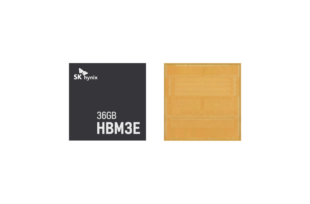
Follow one manufacturer's product line and the trajectory is stark. In 2020, SK hynix mass-produced HBM2E: eight dies, 16GB per stack, 3.6 Gb/s per pin, just over 460 GB/s of bandwidth. HBM3 — the H100 generation — roughly doubled the pin speed to 6.4 Gb/s. By late 2024, HBM3E stacked twelve 3GB dies, each ground 40% thinner so that twelve fit in the height of the old eight: 36GB per cube at 9.6 Gb/s, about 1.2 TB/s per stack.
HBM4, standardized by JEDEC in April 2025 (JESD270-4), is the architectural break. The bus doubles to 2,048 bits, independent channels double to 32, and the spec allows 16-high stacks of 32Gb dies — up to 64GB and 2 TB/s per stack. Vendors are already beating the spec: Samsung's ISSCC 2026 paper demonstrated 13 Gb/s per pin and 3.3 TB/s. Just as important, HBM4 moves the base die from a DRAM process onto a foundry logic node — SK hynix to TSMC's N12, Samsung to its own SF4 — opening the door to custom base dies for Nvidia, OpenAI, AMD, and other hyperscalers.
Now multiply per-stack progress by more stacks per GPU. An A100 in 2020 carried 80GB of HBM2E. Nvidia's Rubin Ultra roadmap, per SemiAnalysis, carries 1,024GB of HBM4E — a 13x jump in per-GPU capacity in roughly six years, every gigabyte of it billed to the AI buildout.
Why memory is half the GPU's bill of materials
SemiAnalysis's bill-of-materials work lands on a startling number: over 50% of an H100's manufacturing cost is HBM, and on Blackwell it grows past 60%. When you buy an 'AI GPU,' you are mostly buying DRAM.
Two forces produce that number. On the demand side stands the memory wall: LLM inference streams every weight for a dense model, or the router-selected active experts (a fraction of the total) for a sparse MoE — plus a KV cache that grows with every token of context — for each token generated, so most inference is bandwidth-bound, not compute-bound. The GPU is quite literally waiting on HBM. No other DRAM delivers the bandwidth, so buyers pay 3x+ per gigabyte over DDR5 with no substitute available.
On the supply side, HBM is the hardest DRAM ever made. Yield compounds with height: even at 99% per bonded layer, an 8-high stack yields 92% and a 12-high only 89% — and reality is worse, because the bigger problem is front-end yield on the TSVs and the power-delivery network that must feed current up through the tower. Every maker runs HBM yields far below its ordinary DRAM.
The economics are perversely elegant: difficulty itself is the moat. Pricing more than makes up for the yield loss, making HBM strongly margin-accretive — the most profitable corner of the DRAM business today (SemiAnalysis); from Ampere to Blackwell Ultra, the single biggest BOM increase is HBM — a wealth transfer from Nvidia's customers to SK Hynix above all. And the treadmill never stops: every capacity bump is immediately consumed by bigger models, so memory is always the next bottleneck.
NAND vs DRAM: two memories, two jobs
One more distinction completes the map. DRAM is working memory: volatile (contents vanish at power-off), byte-addressable, ~100 nanoseconds. NAND flash is storage: non-volatile, read in whole pages, ~100 microseconds — a thousand times slower — but far cheaper per bit; it is what fills SSDs. In an AI datacenter, DRAM and HBM hold the model and the conversation state while computing; NAND holds training datasets, checkpoints, and increasingly the evicted 'cold' context — Nvidia's Dynamo software tiers the KV cache from HBM down to DDR/LPDDR and then to NVMe SSDs. SemiAnalysis's key judgment: these tiers are complements, not substitutes — like L1 cache versus DRAM, more of one does not cannibalize the other.
The structural difference is the more interesting one. NAND solved its own scaling crisis a decade ago by going 3D: a charge-trap cell needs no capacitor, so layers can simply be grown upward — SanDisk/Kioxia's announced BiCS10 will stack 332 of them. DRAM cannot copy this yet, because its capacitor refuses to lie down; that is exactly why HBM stacks finished dies with bumps and TSVs instead of growing layers monolithically, and why '3D DRAM,' expected around 2030-2035, is the technology race that could reshuffle DRAM market share. The investment texture differs accordingly: NAND has five-plus makers and chronically weaker pricing; DRAM has three plus CXMT — and, right now, a once-in-four-decades shortage.

Key Numbers
| Metric | Value | Source |
|---|---|---|
| HBM share of AI GPU manufacturing cost | H100 ~50%+ -> Blackwell ~60%+ | SemiAnalysis — The Memory Wall: Past, Present, and Future of DRAM |
| DRAM density scaling collapse | ~2x over the last decade, vs 2x every 18 months (~100x/decade) in the golden age | SemiAnalysis — The Memory Wall: Past, Present, and Future of DRAM |
| HBM price premium over DDR5 | 3x+ per GB | SemiAnalysis — The Memory Wall: Past, Present, and Future of DRAM |
| HBM stack-yield compounding | 99% per bonded layer -> 92% at 8-high, ~89% at 12-high (real yields degrade faster) | SemiAnalysis — Scaling the Memory Wall: The Rise and Roadmap of HBM |
| HBM2E per stack (2020 volume production) | 16GB (8x 16Gb dies), 3.6 Gb/s per pin, 460+ GB/s per stack | SK hynix Newsroom — SK hynix Starts Mass-Production of High-Speed DRAM 'HBM2E' |
| HBM3E 12-high per stack (2024 volume production) | 36GB (12x 3GB dies, each 40% thinner), 9.6 Gb/s per pin | SK hynix Newsroom — SK hynix Begins Volume Production of the World's First 12-Layer HBM3E |
| JEDEC HBM4 standard (JESD270-4, April 2025) | 2,048-bit interface, up to 8 Gb/s per pin = 2 TB/s per stack; up to 64GB (16-high of 32Gb dies) | TrendForce — JEDEC Finalizes HBM4 Standard, Potentially Easing Pressure on Hybrid Bonding Adoption |
Sources
- SemiAnalysis — The Memory Wall: Past, Present, and Future of DRAM
- SemiAnalysis — Scaling the Memory Wall: The Rise and Roadmap of HBM
- SK hynix Newsroom — SK hynix Starts Mass-Production of High-Speed DRAM 'HBM2E'
- SK hynix Newsroom — SK hynix Begins Volume Production of the World's First 12-Layer HBM3E
- TrendForce — JEDEC Finalizes HBM4 Standard, Potentially Easing Pressure on Hybrid Bonding Adoption
- Wikimedia Commons
- Wikipedia — High Bandwidth Memory (HBM3 6.4 Gbit/s/pin; H100 ships with HBM3)
- SemiAnalysis — AI Capacity Constraints: CoWoS and HBM Supply Chain ('The Real Bottleneck - CoWoS')
- SemiAnalysis — Memory Mania: How a Once-in-Four-Decades Shortage Is Fueling a Memory Boom
- SemiAnalysis — Intel GenAI for Yield, TSMC CFET ('3D DRAM insertion tentatively shown 2030-2035')
- SemiAnalysis — ISSCC 2026: NVIDIA & Broadcom CPO, HBM4 & LPDDR6
- SemiAnalysis — Interconnects Beyond Copper, 1,000 CFETs, SK Hynix Next-Gen NAND
- Wikipedia — Memory refresh
- Wikipedia — Memory hierarchy (latency table)
Related sector deep-dives
Optional — jump ahead if this module is all you needed; otherwise continue the ladder above.