One Computer, Two Networks
Training a frontier model does not happen on 'a GPU'; it happens on tens of thousands of GPUs that must behave like a single machine. The awkward truth is that no single network can do that job, so every AI datacenter runs two networks with opposite designs and opposite economics.
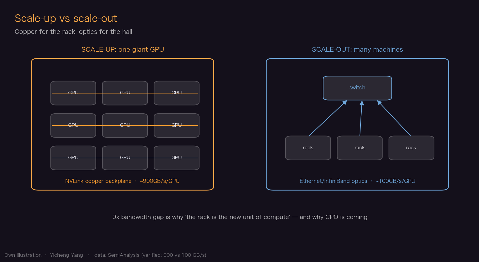
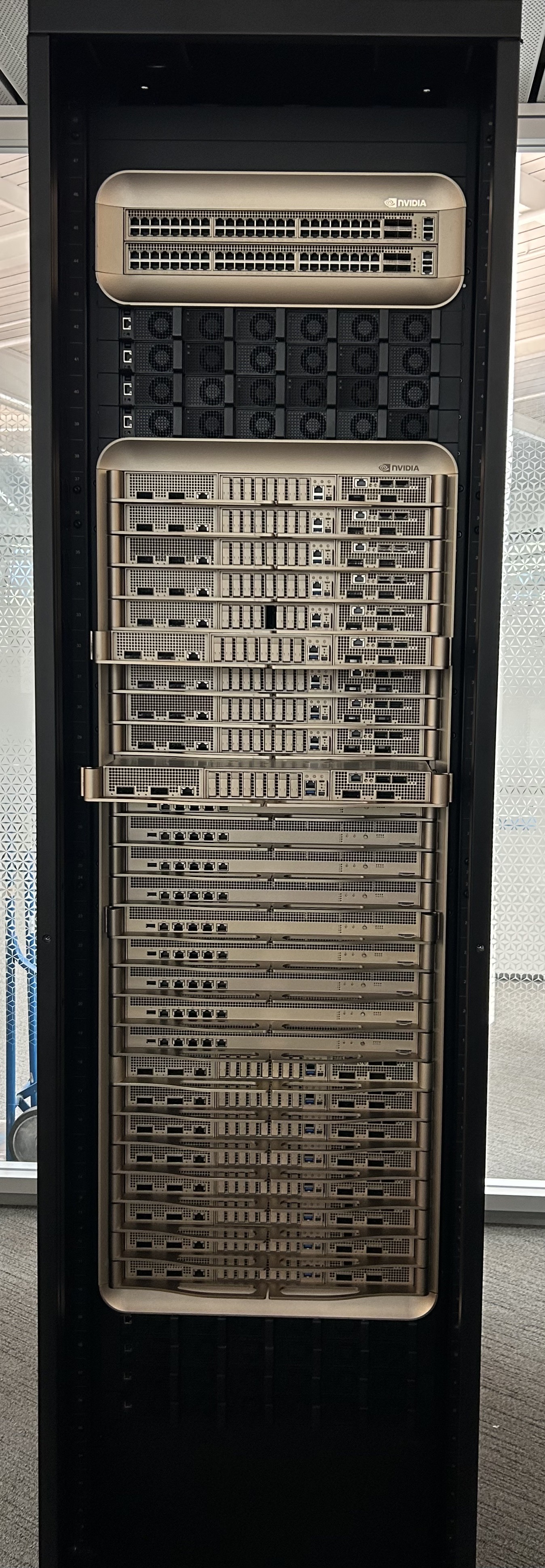
The first is scale-up. Take one rack: Nvidia's GB200 NVL72 wires 72 GPUs together so tightly — every GPU can talk to every other GPU at 900 GB/s, within an order of magnitude of how fast a GPU talks to its own memory — that software can treat the whole rack as one giant GPU. This domain is the NVLink domain, and the number of GPUs inside it (72 here) is called the 'world size'. Think of it as one open-plan office: anyone can shout across the desks and be heard instantly.
The second is scale-out. To go beyond one rack, you stitch thousands of racks together with InfiniBand or Ethernet — the same family of technology as ordinary datacenter networking, hardened for AI. Per GPU, this fabric carries about 50 GB/s on the original GB200 (a 400G ConnectX-7 NIC) — roughly one-eighteenth of scale-up — rising to about 100 GB/s, or one-ninth, on the 800G (GB300-generation ConnectX-8) NIC. It is the postal system between office buildings: enormous total capacity, but data gets packaged up and waits its turn.
Why tolerate a 9-to-18x gap instead of making everything fast? Because the chatter is not uniform. Splitting a single matrix multiplication across chips (tensor parallelism) requires constant, latency-critical exchange — that traffic must live on scale-up. Synchronizing gradients between whole copies of a model (data parallelism) happens far less often and tolerates the slower fabric. The art of cluster design is matching each kind of traffic to the cheapest network that can carry it.
The Bandwidth Math: 900 vs 100 (and the Bits-vs-Bytes Trap)
First, the unit trap that catches every newcomer: networking people speak in bits per second (Gbit/s), chip people in bytes per second (GB/s), and 8 bits = 1 byte. So the 800G ConnectX-8 NIC attached to each GB300-generation Blackwell GPU (the original GB200 shipped a 400G ConnectX-7) means 800 Gbit/s = 100 GB/s, while NVLink 5 gives each GPU 7.2 Tbit/s = 900 GB/s of scale-up bandwidth (Nvidia's marketing figure of '1.8 TB/s' counts both directions at once). That is the 9x gap, computed in one line.
Now the roadmap. Rubin's NVLink 6 doubles scale-up to 14.4 Tbit/s per GPU; scale-out doubles to 1.6 Tbit/s not via a faster NIC but by giving each GPU two 800G ConnectX-9 NICs. Meanwhile HBM memory feeds each GPU at roughly 8 TB/s. Notice the hierarchy: memory ≈ 8,000 GB/s, scale-up ≈ 900, scale-out ≈ 100. Each step down the ladder loses roughly an order of magnitude — and each step is a place where a badly placed communication pattern leaves million-dollar silicon sitting idle, which is why engineers obsess over 'keeping traffic on the fast tier'.
This hierarchy also explains the industry's obsession with world size. When the NVLink domain jumped from 8 GPUs (H100 generation) to 72 (GB200), mixture-of-experts models — whose all-to-all traffic between experts is brutal — could suddenly keep that chatter entirely on the fast tier. A bigger world size is worth real money in training throughput, which is exactly why the fight over what physically carries it — copper or light — is the central drama of this module.
Why Copper Refuses to Die: Within Two Meters, Copper Is King
A copper wire is the cheapest, most reliable, lowest-power way to move bits — as long as the distance is short. The physics is simple: the faster you toggle a signal, the more the wire attenuates and smears it. At today's 200 Gbit/s-per-lane speeds, a passive copper cable is good for only about 2 meters. Conveniently, a rack is about 2 meters tall.
So Nvidia built the NVL72's spine entirely of copper: 5,184 differential pairs run through a backplane connecting 72 GPUs to the NVLink switch chips. Copper needs no laser and no photodetector, and adds essentially zero power. SemiAnalysis ran the counterfactual: building that same spine with optics would take 648 1.6T optical transceivers, roughly $550k of extra bill-of-materials and ~20 kW of extra power per rack. 'One giant GPU' is buildable today precisely because it is built of copper.
Two definitions make copper's limits legible. A SerDes (serializer/deserializer) is the circuit at the edge of every chip that converts wide, slow internal data into one blistering-fast serial stream — the chip's mouth and ears; its per-lane speed (112G, now 224G) sets how much data each wire can carry. NVLink's bandwidth grew 11x over five generations almost entirely by speeding up the SerDes, not by adding wires. But the next doubling — 224G to 448G per lane — is in genuine trouble: it likely requires new modulation schemes (PAM6/PAM8), and reach shrinks further still. Nvidia's Rubin-generation '448G' is actually a clever dodge: transmitting 224G in each direction simultaneously over the same wire pair, using echo cancellation — the same trick as a telephone line. When SerDes stops improving while copper's reach keeps shrinking, world sizes can no longer grow inside copper. That is the opening for optics — and, SemiAnalysis argues, a crack in Nvidia's NVLink moat that AMD and the hyperscalers fully intend to widen.
Optics: Pluggables → LPO → CPO
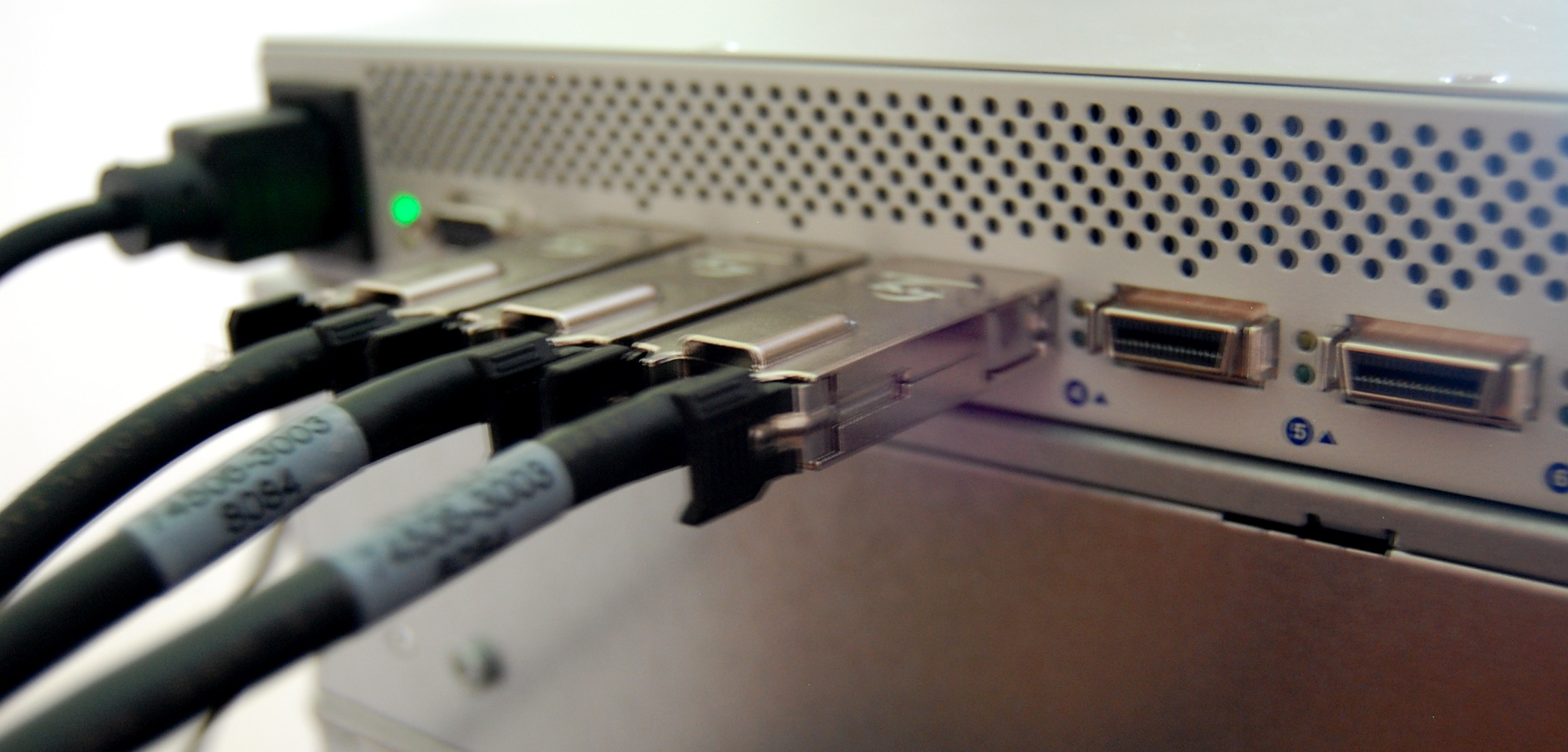
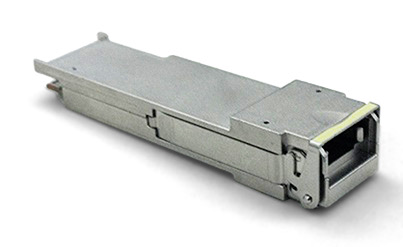
Beyond roughly 2 meters, you must convert electrons into photons. Today that is done with pluggable transceivers: thumb-sized modules slotted into switch faceplates, each containing a laser, a modulator (which writes bits onto light), and a DSP chip that cleans up and retimes the electrical signal. A large cluster contains hundreds of thousands of them, and they dominate scale-out economics: about 60% of scale-out networking cost sits in these modules, and the DSP alone eats ~50% of an 800G module's power and 20-30% of its bill of materials — the DSP is regarded as public enemy number one of cost and power, as SemiAnalysis reports.
The industry's answer is a three-step progression. LPO (linear pluggable optics) keeps the pluggable form factor but deletes the DSP, letting the switch chip's own SerDes drive the optics directly — cheaper and cooler, but engineering-fragile, and adoption has lagged predictions. CPO (co-packaged optics) goes further: it moves the optical engine onto the same package as the switch or GPU silicon, shrinking the electrical path from ~20 centimeters to millimeters. With no DSP and no long, lossy trace, optical-link energy falls 65-73%.
Here is the nuance most headlines miss. In scale-out, CPO's savings dilute to a rounding error — networking is only ~9% of cluster power, so CPO saves just 2-4% of cluster power and 3-7% of cluster cost. Against that stand real fears: a failed pluggable is hot-swapped in minutes, while a failed CPO engine takes the whole switch down with it — and 80% of returned pluggable modules turn out to be 'no trouble found' anyway. The real prize is scale-up: optics removes copper's 2-meter leash, letting the 'one giant GPU' span many racks. That is why CPO's true arrival is tied to Rubin Ultra/Feynman and AWS's Trainium 4 late this decade, not to today's Ethernet switches.
Either way, reliability is the gate: on a 100,000-GPU cluster, flaky optical links produce the first training-job failure in roughly 26 minutes. What hyperscalers are actually buying is not speed — it is uptime.
Who Sells What: Reading the Market Map
With the mechanisms in hand, the vendor map reads itself. Nvidia owns scale-up — NVLink is the moat — and sells both flavors of scale-out (Quantum InfiniBand and Spectrum-X Ethernet; the Ethernet flavor has grown to rough parity with InfiniBand). Broadcom is the anti-Nvidia bet: hyperscalers buy its Tomahawk switch chips to escape the 'Nvidia tax', it shipped the first production CPO switches, and it co-designs Google's TPU. Marvell dominates the DSP — precisely the chip the whole industry is trying to delete — which is why it paid billions for Celestial AI to leap directly to scale-up CPO. Transceiver assemblers (InnoLight, Eoptolink, Fabrinet, Coherent) ride GPU unit growth; the recurring 'optics demand will collapse' scare is wrong because every GPU still ships with its scale-out ports — copper only ever displaced optics inside the rack. Copper itself is Amphenol's franchise (the NVLink backplane). TSMC quietly won CPO integration with its COUPE packaging platform. And the standards fights — Ethernet/UEC versus InfiniBand for scale-out, UALink/SUE versus NVLink for scale-up — are all the same story told twice: an industry trying to commoditize what Nvidia keeps proprietary.

.jpg)

Key Numbers
| Metric | Value | Source |
|---|---|---|
| NVLink 5 scale-up bandwidth per GPU | 900 GB/s (7.2 Tbit/s) — 9x the 800 Gbit/s scale-out link | SemiAnalysis — Co-Packaged Optics (CPO) Book – Scaling with Light |
| Passive copper reach at 200G/lane | ~2 m — caps the NVLink domain at 1-2 racks | SemiAnalysis — Co-Packaged Optics (CPO) Book – Scaling with Light |
| GB200 NVL72 copper NVLink spine vs the optical counterfactual | 5,184 copper differential pairs; optics would need 648 1.6T transceivers, ~$550k BoM & ~20 kW per rack | SemiAnalysis — GB200 Hardware Architecture - Component Supply Chain & BOM |
| DSP share of an 800G pluggable module | ~50% of power / 20-30% of BoM | SemiAnalysis — Co-Packaged Optics (CPO) Book – Scaling with Light |
| CPO optical-link energy saving vs DSP pluggable | 65-73% | SemiAnalysis — Co-Packaged Optics (CPO) Book – Scaling with Light |
| CPO saving after cluster-level dilution (scale-out) | 2-4% of cluster power / 3-7% of cluster cost | SemiAnalysis — Co-Packaged Optics (CPO) Book – Scaling with Light |
| Copper vs optical link reliability (MTTF) | optical NIC-to-leaf links ~5-yr MTTF each -> first job failure in ~26 min at 100k GPUs; DAC copper markedly more reliable (fewer link flaps) | SemiAnalysis — 100,000 H100 Clusters |
Sources
- SemiAnalysis — Co-Packaged Optics (CPO) Book – Scaling with Light
- SemiAnalysis — GB200 Hardware Architecture - Component Supply Chain & BOM
- SemiAnalysis — 100,000 H100 Clusters
- Wikimedia Commons (CC BY-SA 4.0, User:Pokiiri)
- Wikimedia Commons (CC BY 2.0, ChrisDag)
- Wikimedia Commons (CC BY-SA 3.0, Jesseschulman)
- NVIDIA — GB200 NVL72 product page ('1.8 TB/s of GPU-to-GPU interconnect')
- NVIDIA — DGX B200 page (64 TB/s HBM3e bandwidth across 8 GPUs = 8 TB/s per GPU)
- Broadcom press release — 'Broadcom Delivers Industry's First 51.2-Tbps Co-Packaged Optics Ethernet Switch Platform' (Bailly)
- Marvell Technology Form 8-K, Dec 2 2025 (SEC EDGAR) — Celestial AI acquisition and Amazon warrant agreement
- SDxCentral / IDC — 'Nvidia tops Ethernet data center switch charts by revenue as sales soar' (June 22, 2026)
Related sector deep-dives
Optional — jump ahead if this module is all you needed; otherwise continue the ladder above.