A transistor is a switch: two hundred billion faucets on your thumbnail
Strip away every layer of the AI story — the models, the GPUs, the datacenters — and at the bottom you find one device repeated trillions of times: the transistor. A transistor is an electrically controlled switch with three terminals. Current flows from the source to the drain, and the gate sits on the channel between them like the handle on a faucet. Put a small voltage on the gate and the channel conducts — the faucet opens, and that is a '1'. Remove the voltage and the channel blocks — a '0'. That is genuinely all it does.
Everything else is assembly. Wire a few switches together and you get a logic gate (an AND, an OR); wire logic gates together and you get an adder; keep going and you get a CPU, a GPU, a memory chip. A modern AI GPU packs roughly two hundred billion of these faucets, each flipping billions of times per second.
Why the fifty-year obsession with making them smaller? Because shrinking a transistor used to improve everything at once: smaller switches meant more of them per chip (more capability), shorter distances for electrons to travel (more speed), less charge to move on each flip (less energy) — and, crucially, a lower cost per switch, because a chip's cost is mostly the silicon area it occupies. One knob, four wins. That free lunch, and how it ended, is the subject of this module.
Moore's Law was always an economic law, not a physical one
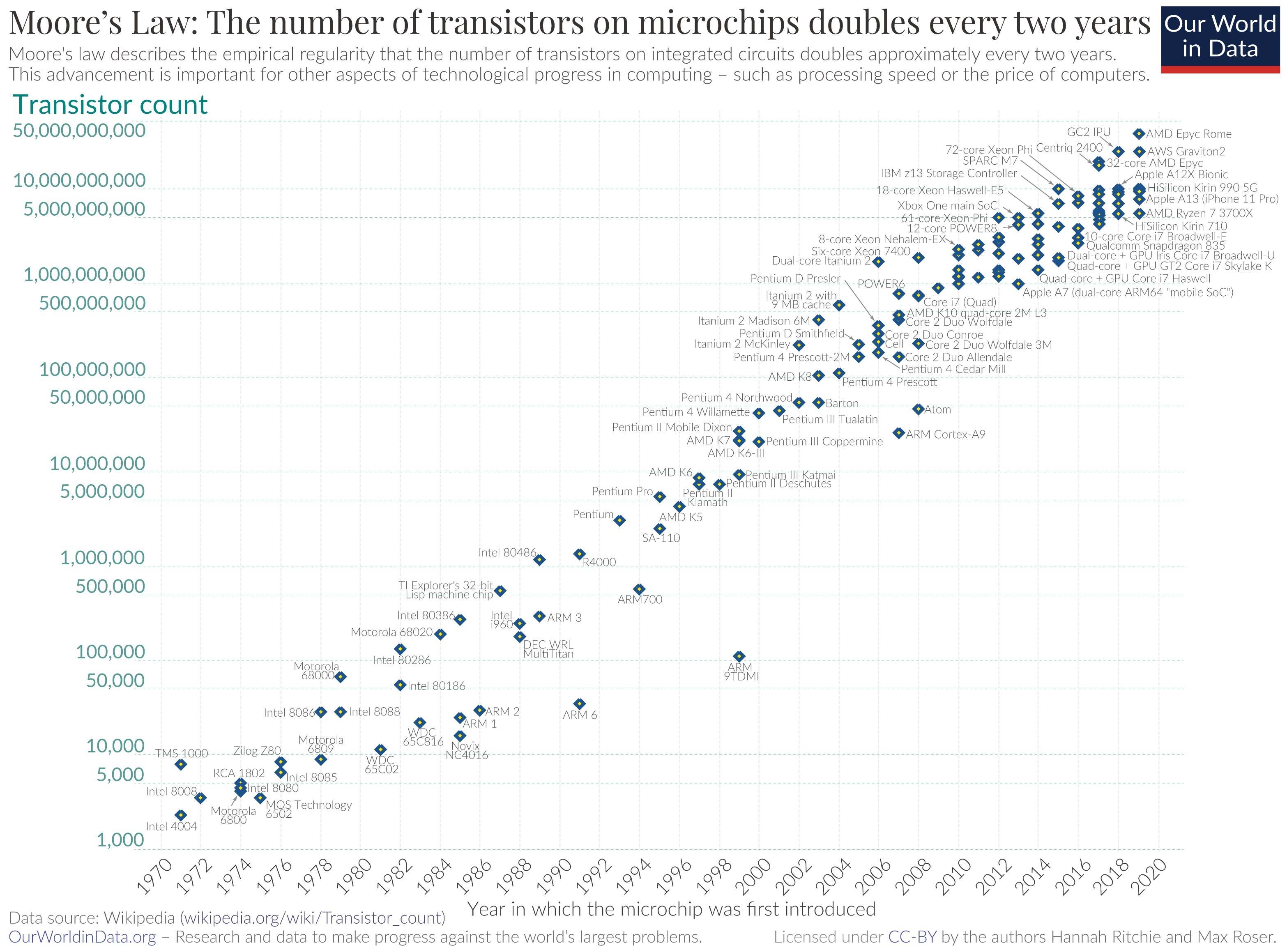
In 1965, Gordon Moore observed that the number of components you could put on a chip at the lowest cost per component had been doubling every year, and predicted it would continue (he later revised the cadence to every two years). Read the phrasing carefully: Moore's Law was never 'transistors get smaller' — it was 'the cost-minimizing complexity doubles.' It is a claim about a cost curve.
No equation of nature enforces it. It held because the industry made it hold: every couple of years, finer lithography let foundries print roughly twice as many transistors on the same wafer area, and as long as wafer cost rose more slowly than density, each transistor got substantially cheaper per node. Cheaper transistors meant designers could afford twice as many, so chips got dramatically more capable at flat prices, which grew the market, which funded the next, more expensive generation of fabs. Moore's Law is best understood as a self-fulfilling prophecy — a coordination device telling chip designers, toolmakers and software companies what to expect and when.
Keep this economic reading in mind, because it defines what 'the end of Moore's Law' actually means. Transistors are still shrinking today. The question that matters for every company in this series is whether they are still getting cheaper — and since the 3nm generation, the honest answer is: barely.
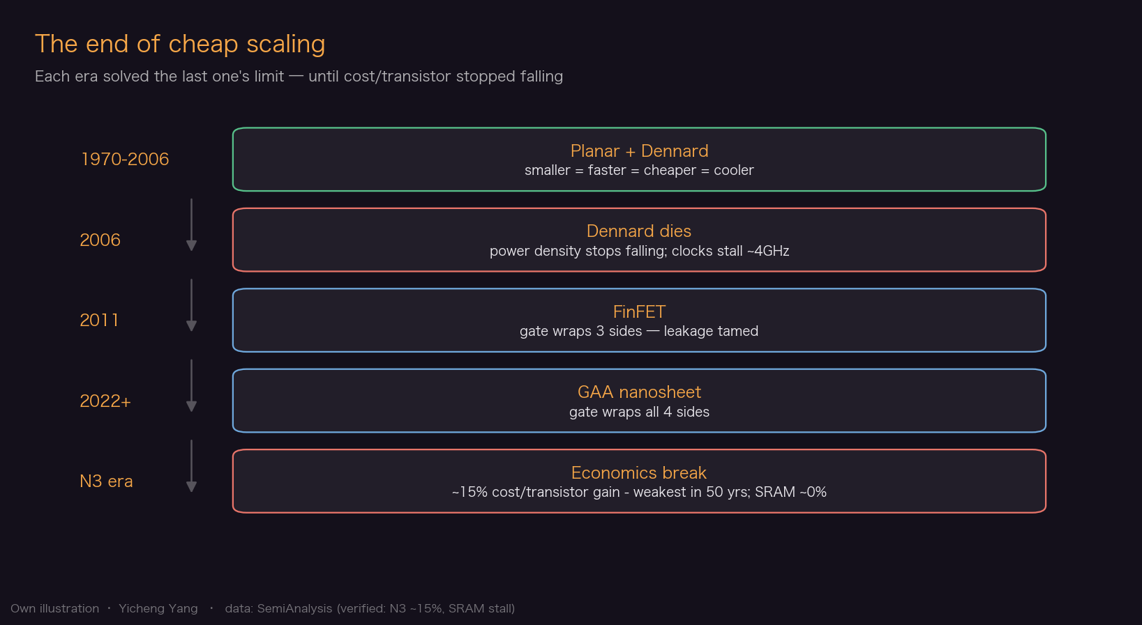
Dennard scaling: the physics free lunch that died around 2005
Moore's Law had a quieter twin that did much of the heavy lifting. In 1974, IBM's Robert Dennard showed that if you shrink every dimension of a transistor by the same factor and reduce its operating voltage proportionally, the chip's power density stays constant: a new chip with twice the transistors, each running faster, burns no more watts per square millimeter than its predecessor. This is why, for three decades, every node delivered transistors that were simultaneously smaller, faster, cooler and cheaper — no design ingenuity required. CPU clock speeds climbed from megahertz to gigahertz essentially for free.
Around 2005, the voltage part of the recipe hit a floor. Transistors need a minimum voltage to switch reliably, and as channels became tiny, current began leaking through even when the switch was 'off' — the faucet dripped. Once voltage stopped scaling, every further shrink raised power density instead of holding it constant, and chips slammed into thermal limits: clock speeds froze in the 3-5 GHz range, where they remain two decades later.
The industry's response reshaped computing twice. First came multicore (roughly 2005-2020): if you cannot make one core faster, put several slower ones on the die. Then came specialization: build narrow hardware that does one thing extremely efficiently — the opening GPUs and AI accelerators drove through. Dennard's death is also the deep reason performance-per-watt became the industry's binding metric, and why, far downstream, electricity is now a top constraint on AI (see the datacenter power module).
Planar → FinFET → GAA: a three-dimensional war on leakage
The leakage that killed Dennard scaling set off a twenty-year redesign of the transistor's geometry, with one goal: give the gate more control over the channel so the switch shuts off properly.
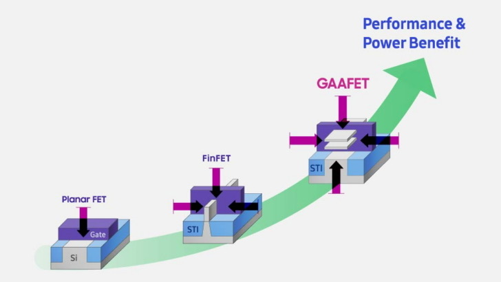
The original planar transistor — the dominant design into the early 2010s — lays the channel flat on the silicon surface, the gate touching one side only. Below roughly the 28nm generation, that single-sided grip becomes too weak: electrons sneak beneath the gate's reach. The FinFET, adopted from 22nm (around 2011) onward, raises the channel into a thin vertical fin so the gate drapes over it on three sides — a far firmer grip, much less leakage, and another decade of scaling. But fins are rigid: their height is fixed by the process, and by the 3nm generation engineers had run out of ways to improve them. Gate-all-around (GAA) is the endgame of this logic: the channel becomes a stack of horizontal nanosheets, each completely surrounded by the gate on all four sides, and designers can vary sheet width to trade drive strength against density. The 2nm-generation nodes — TSMC N2, Intel 18A, Samsung SF2 — are all GAA, arriving 2025-2026. Intel 18A pairs GAA with a second change — backside power delivery (~15-20% power benefit; the first interconnect paradigm shift since copper in 1997) — which TSMC and Samsung follow with A16 (2026) and SF2Z (2027).
One habit to build now: node names like '3nm' and '2nm' are marketing labels, not measurements — nothing on an N3 chip is actually 3 nanometers. Compare nodes on density, power and cost, never on the name.
The number that broke: cost per transistor — and SRAM's dead stop
Now put the economics and the physics together, and look at what happened at TSMC's 3nm.
N3 raised total spend per wafer-start by 38-55% versus N5 — EUV lithography layers nearly doubled on the first version, each layer another pass through machines costing hundreds of millions of dollars. Density rose about 56%, but only in the best configuration; typical designs saw around 30%. With wafer cost climbing that fast against only a modest density gain, the two roughly cancel: SemiAnalysis puts the improvement in cost per transistor at only ~15% in the best case — the weakest scaling for a major node in the industry's fifty-plus-year history — and roughly zero for the average design. The deflation engine that had made each generation of computing cheaper than the last had, for practical purposes, stalled.
Inside that average hides something worse. SRAM — the six-transistor memory cell used for on-chip cache, often around a third of a modern processor's area (30% SRAM in SemiAnalysis's standard monolithic chip mix), and approaching half in cache-heavy designs — stopped shrinking entirely: the high-density SRAM cell on N3E measures 0.021 µm², identical to N5. SRAM cells need matched, noise-tolerant transistors and cannot use the layout tricks that keep logic scaling, so each new node now shrinks the logic while dragging the cache along at full size. Chip-level gains are therefore even weaker than the headline transistor numbers suggest.
The investor translation: paying up for N3 or N2 buys power efficiency and density — which AI desperately needs — but it no longer buys cheaper transistors. Compute demand began exploding at precisely the moment compute's unit cost stopped falling. Everything in the AI supply chain follows from that collision.
What the industry does instead: package, stack, co-design
When optimization at the transistor level saturates, you move the optimization up a level. The industry's answer has three prongs — and they are, not coincidentally, the next several sectors in this series.
First, advanced packaging and chiplets. If big monolithic dies on the newest node no longer pay, split the design: put only the logic that truly benefits on N3/N2, keep cache and I/O on older, cheaper nodes, and reconnect the pieces with packaging so dense the assembly behaves like one chip. There is also a bandwidth reason: transistor density doubles every two years, but the data rate off a chip doubles only every four — so moving signals between chips is the scarcer resource, and packaging attacks exactly that. TSMC's CoWoS platform, which mounts GPUs and their memory on a silicon interposer, generated $9.6B of revenue in 2025; advanced packaging is now over a tenth of TSMC's revenue and frequently the binding constraint on AI accelerator supply.
Second, memory. With SRAM frozen and DRAM scaling slow, capacity comes from stacking: HBM piles DRAM dies vertically and places them millimeters from the GPU — the defining commodity of the AI era (see the memory & HBM module).
Third, co-design. Nvidia now buys 'Moore's Law' at the system level: larger NVLink domains (72 GPUs acting as one), lower-precision arithmetic (FP8, then FP4), and software that extracts more from the same silicon. Performance per rack still doubles on schedule — but it is paid for in dollars, watts and engineering, not by free physics. That is the single most important lens for everything that follows.

Key Numbers
| Metric | Value | Source |
|---|---|---|
| N3 cost-per-transistor improvement vs N5 | ~15% (best case) — weakest scaling for a major node in 50+ years | SemiAnalysis — TSMC's 3nm Conundrum, Does It Even Make Sense? |
| N3 total spend per wafer-start vs N5 | +38-55% (density +56% only in the best FinFlex config; most designs ~30%) | SemiAnalysis — TSMC's 3nm Conundrum, Does It Even Make Sense? |
| SRAM high-density bitcell size, N5 vs N3E | 0.021 µm² — identical (zero shrink) | SemiAnalysis — TSMC's 3nm Conundrum, Does It Even Make Sense? |
| Dennard scaling era (constant power density while shrinking) | Formulated 1974 (IBM, Robert Dennard) → ended around 2005 | SemiAnalysis — A Century of Moore's Law |
| Backside power delivery benefit at 2nm-generation nodes | ~15-20% power improvement; first interconnect paradigm shift since copper (1997) | SemiAnalysis — Clash of the Foundries: Gate All Around + Backside Power at 2nm |
| TSMC CoWoS advanced-packaging revenue (2025) | $9.6B — 2.5x InFO; advanced packaging >10% of TSMC revenue | SemiAnalysis — Apple-TSMC: The Partnership That Built Modern Semiconductors |
| Transistor density vs chip IO (off-chip bandwidth) scaling | 2x every 2 years vs 2x every 4 years | SemiAnalysis — Advanced Packaging Part 1 – Pad Limited Designs |
Sources
- SemiAnalysis — TSMC's 3nm Conundrum, Does It Even Make Sense?
- SemiAnalysis — A Century of Moore's Law
- SemiAnalysis — Clash of the Foundries: Gate All Around + Backside Power at 2nm
- SemiAnalysis — Apple-TSMC: The Partnership That Built Modern Semiconductors
- SemiAnalysis — Advanced Packaging Part 1 – Pad Limited Designs
- Our World in Data (Hannah Ritchie & Max Roser), CC BY 4.0, via Wikimedia Commons
- Samsung Newsroom
- NVIDIA Newsroom — NVIDIA Blackwell Platform Arrives (B200: 208 billion transistors)
- Wikipedia — Moore's law (1975 revision to doubling every two years)
- Intel — 22nm Tri-Gate Technology Backgrounder
- Samsung Newsroom — Samsung Begins Chip Production Using 3nm Process Technology With GAA Architecture (June 30, 2022)
- Karl Rupp — 50 Years of Microprocessor Trend Data (frequency plateau)
Related sector deep-dives
Optional — jump ahead if this module is all you needed; otherwise continue the ladder above.