Step Zero: From Beach Sand to a Perfect Crystal
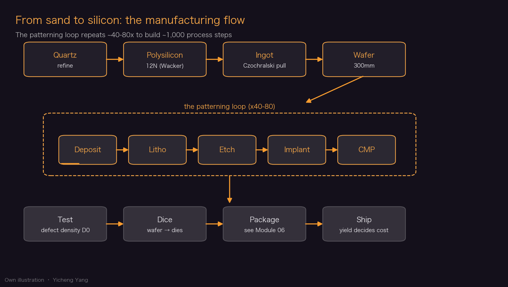
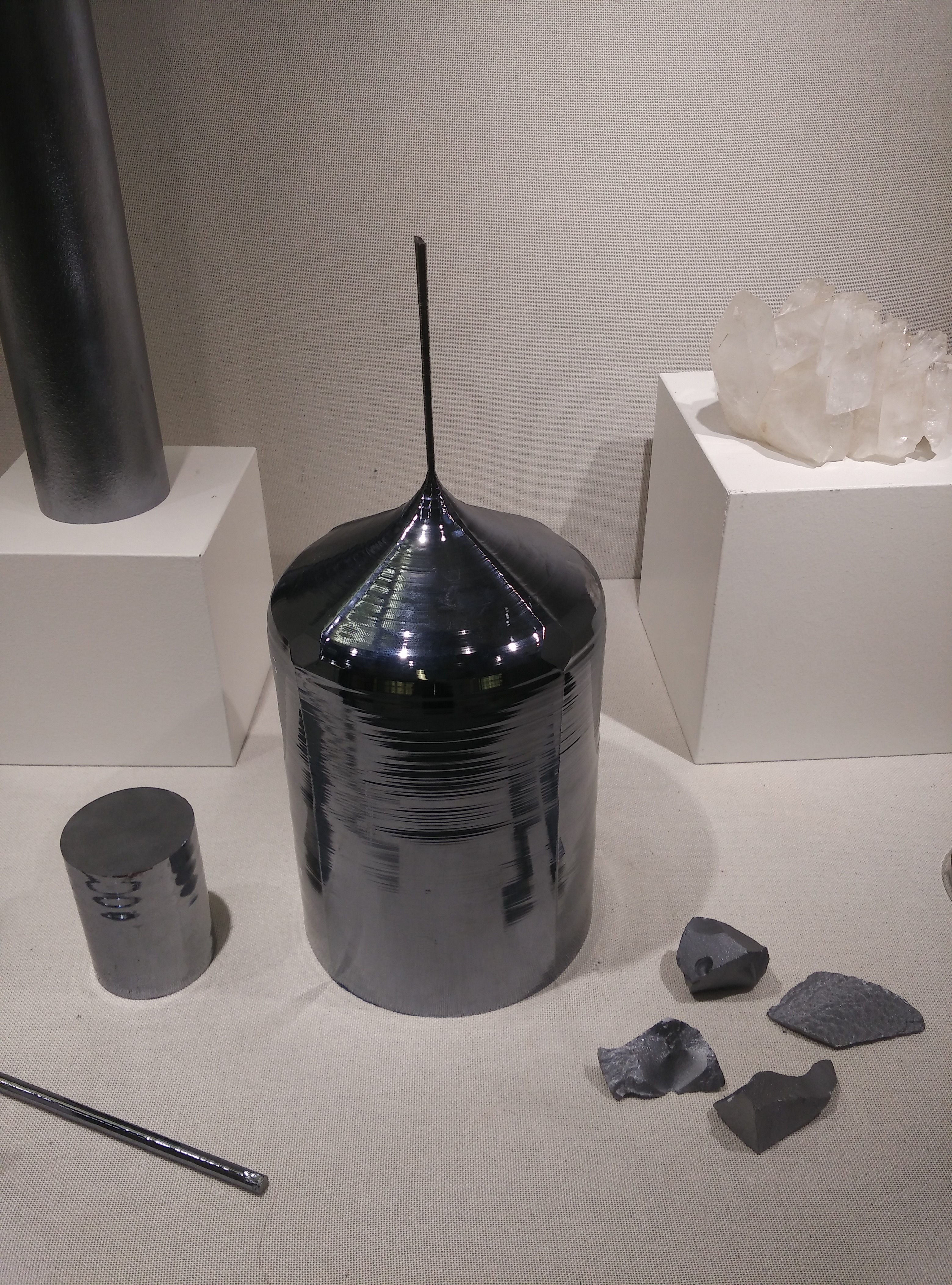
Every chip begins as quartz — silicon dioxide, the main mineral in ordinary sand. Smelting quartz with carbon in an arc furnace yields 'metallurgical-grade' silicon, roughly 98–99% pure. That sounds clean; for electronics it is filth. A transistor works by deliberately adding a tiny number of impurity atoms ('dopants') to silicon to control exactly how it conducts. The trick only works if the background material is almost perfectly empty: a stray phosphorus or boron atom in the wrong place is indistinguishable from an intentional one. So raw silicon is converted into a gas (trichlorosilane), distilled like whiskey to strip out contaminants, then re-deposited as hyperpure polysilicon. Wacker, one of the leading producers, ships semiconductor-grade polysilicon at better than 99.9999999999% purity — critical impurities measured in parts per trillion.
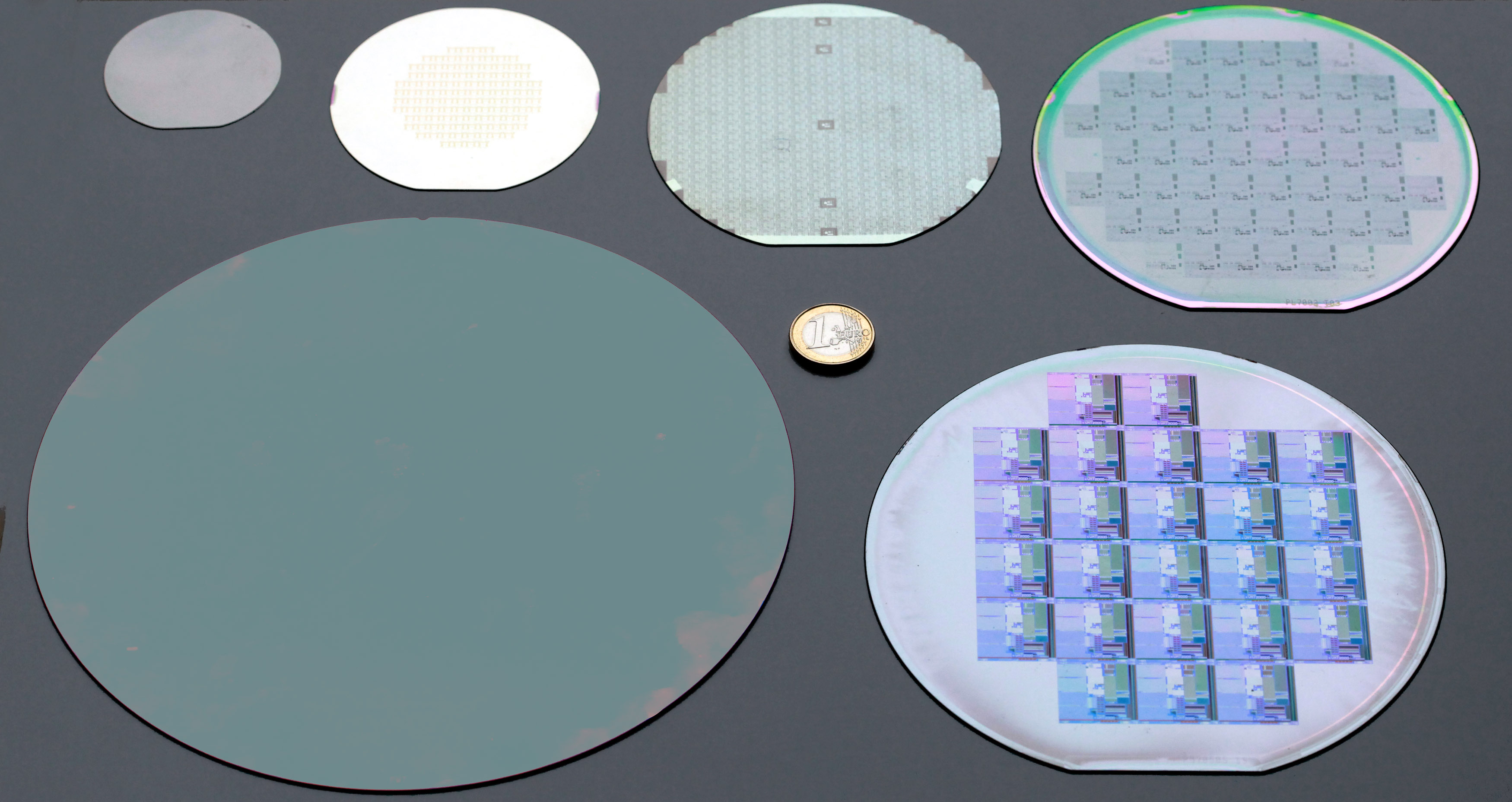
Purity alone is not enough; the atoms must also line up. Polysilicon is a jumble of small crystals, and the boundaries between grains scatter electrons, making every transistor behave slightly differently. The fix is the Czochralski process: melt the polysilicon at about 1,414°C, dip a small seed crystal into the melt, and pull it upward slowly while rotating. Atoms freeze onto the seed in perfect crystalline order, growing a single flawless crystal — a mirror-gray ingot up to 300mm in diameter and a couple of meters long. Diamond wire saws then slice the ingot into discs under a millimeter thick, which are ground and polished until the surface is flat to within atoms. That 300mm mirror is the canvas. Every GPU and every HBM stack in this series is drawn on one.
The Fab Loop: Building a Skyscraper with Light and Stencils
A finished chip is not a flat drawing but a three-dimensional city: transistors occupy the ground floor, with fifteen or more levels of copper wiring stacked above like highway interchanges. The fab builds it one layer at a time, looping through five basic verbs:
Deposit — lay an ultra-thin, uniform film (insulator, metal, or silicon) over the whole wafer; the finest films are grown one atomic layer at a time (ALD). Pattern — coat the wafer with light-sensitive photoresist and project this layer's design through a photomask, a quartz stencil, shrinking the image 4x onto the wafer. The most advanced machines (EUV) do this with 13.5nm-wavelength light. Etch — use plasma or chemicals to eat away material wherever the developed resist leaves it exposed, transferring the pattern from resist into film. Implant — fire dopant ions into selected regions to create the electrically active hearts of the transistors, then anneal at high temperature to heal the crystal. Polish (CMP) — grind the surface flat with a chemical slurry so the next layer starts on a plane.
Then repeat. A leading-edge process uses more than 60 lithography layers, and each carries its own cluster of deposition, etch, clean, and metrology steps; Intel has shown a single metal-wiring scheme that alone required three EUV exposures and over 40 process steps. In total a wafer traverses on the order of a thousand steps over roughly three months of around-the-clock processing — and an error at step 700 scraps the previous 699. What is genuinely hard to copy about a fab is not any single machine; it is the proven recipe for running a thousand steps in a row without failing.
What a 'Node' Actually Is — and Why '3nm' Measures Nothing
'3nm' sounds like a measurement. It isn't. A process node is a complete, frozen, qualified recipe — the full combination of masks, materials, machine settings, and design rules that a fab sells capacity on. Nothing on a '3nm' chip is 3nm wide; the tightest metal lines sit 20–30nm apart. The numbers that actually mean something are pitches (how closely gates and wires can be packed), the transistor density they produce, and PPA — performance, power, area. Each node also spawns a family of variants (N3B, N3E, N3P, N3X…) tuned toward cost, phones, or high-performance computing.
Nodes matter economically because for fifty years each new one made transistors cheaper — that was the commercial engine of Moore's Law. The engine is now sputtering. SemiAnalysis's cost model of TSMC's 3nm found cost per transistor improving only ~15% versus 5nm in the best case — the weakest scaling of any major node in more than fifty years — while a single 3nm photomask set costs about $40M, versus over $10M at 7nm and around $1M at 28nm. Design costs balloon alongside. Three consequences follow: fewer and fewer companies can afford leading-edge designs at all; value migrates toward chiplets and advanced packaging, which squeeze more out of existing transistors (Module 04 territory); and node names have become marketing weapons in the TSMC–Intel–Samsung race, where the honest scorecard is density, power, and cost — not the number in the brand (Sector Brief 02).
Yield: The Exponential That Rules Chip Economics
Picture the wafer as a sheet of postage stamps; each stamp is one die, the rectangle that becomes a chip. Defects — a particle that landed mid-process, an etch a nanometer too deep — scatter across the wafer roughly at random, with an average defect density called D0 (defects per cm²). One killer defect usually means one dead die. The math is merciless: die yield ≈ e^(−area × D0), exponential in die area. Small dies slip between the defects; big dies are targets. Double the area and your survival probability squares: if a small chip yields 90% on a given line, a chip four times its size yields about 66% at the same D0. AI GPUs live at the extreme — nearly all are designed against the ~858mm² 'reticle limit,' the largest area one exposure can print — so early in a node's life their yields can sit below half.
Three consequences. First, yield learning is the business: a node launches with high D0 that falls for years, which is why margins on a new node start ugly and improve — and why TSMC's aggressive N3B struggled while the relaxed N3E that replaced it showed, in TSMC's words, consistently healthier defect density. Second, giant dies pay a superlinear area tax — a core reason AI silicon is moving to chiplets: split one huge die into several small ones that each yield well, then reassemble them inside the package. Third, salvage: designs carry spare cores and memory so a partially defective die can be sold, bad blocks disabled, as a cheaper SKU.
Cleanrooms and the $20 Billion Ticket
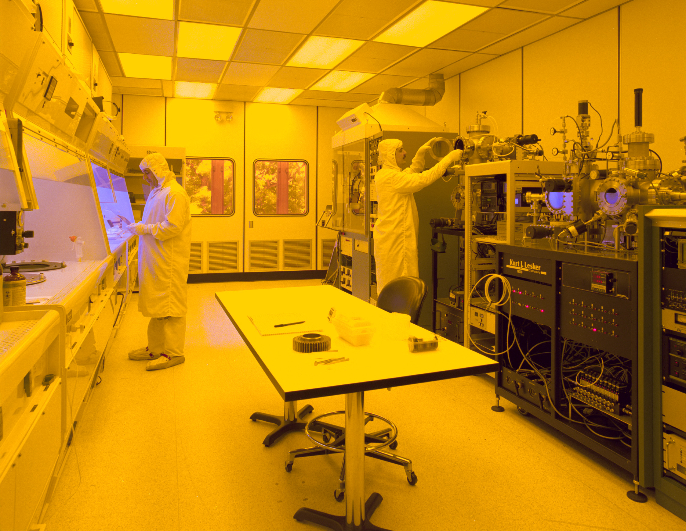
Because one invisible particle can kill a die, the fab must be among the cleanest places humans have ever built. Cleanroom air is scrubbed by wall-to-wall filtration until it holds orders of magnitude fewer particles than a hospital operating room; wafers travel in sealed pods (FOUPs) carried by overhead robots; people — the dirtiest objects in the building — wear full-body 'bunny suits' and touch nothing.
Yet the cleanroom shell is the cheap part. The money is in the tools that fill it. A single EUV lithography machine sells for about $225M and can pattern more than $650M worth of finished wafers per year; lithography alone consumes ~35% of the cost of a 3nm process. Fill a building with hundreds of such tools and, by Intel's own arithmetic, a leading-edge fab costs $25–30B per 10,000 wafers per week of capacity — TSMC has quoted roughly $42B for its Arizona 3nm capacity. TSMC's total planned US investment — three additional fabs, two advanced packaging plants, and an R&D center on top of the original $65B three-fab Phoenix site — comes to $165B.
The economics follow directly. A fab's cost is mostly depreciation, which burns whether or not wafers move, so fabs must run flat-out around the clock; swings in utilization pass almost one-for-one into profit — that is foundry cyclicality. And each generation's fab costs more than the last, so only firms with locked-in demand for the next node can fund the next fab. That flywheel built the most concentrated critical industry on earth — the subject of Sector Brief 02.



Key Numbers
| Metric | Value | Source |
|---|---|---|
| Semiconductor-grade polysilicon purity | >99.9999999999% (critical impurities in parts per trillion) | Wacker Chemie AG — press release, Jul 17, 2025 |
| EUV lithography tool economics | $225M per tool → >$650M of finished wafers per year | SemiAnalysis — How to Kill 2 Monopolies with 1 Tool |
| Lithography share of 3nm process cost | ~35% | SemiAnalysis — EUV Requirements Halved? Applied Materials' Sculpta Redefines Lithography And Patterning |
| Photomask set cost by node (28nm → 7nm → 3nm) | ~$1M → >$10M → ~$40M; leading edge uses >60 lithography layers | SemiAnalysis — The Dark Side Of The Semiconductor Design Renaissance |
| N3 cost-per-transistor improvement vs N5 | ~15% best case — weakest major-node scaling in 50+ years | SemiAnalysis — TSMC's 3nm Conundrum, Does It Even Make Sense? |
| Leading-edge fab capital cost | $25–30B per 10,000 wafers/week (Intel); TSMC quoted ~$42B for Arizona 3nm | SemiAnalysis — Is Intel Back? Foundry & Product Resurgence Measured |
| TSMC total planned US investment | US$165B — 3 new fabs + 2 advanced packaging plants + R&D center, on top of the $65B three-fab Phoenix site | TSMC — press release, Mar 4, 2025 |
Sources
- Wacker Chemie AG — press release, Jul 17, 2025
- SemiAnalysis — How to Kill 2 Monopolies with 1 Tool
- SemiAnalysis — EUV Requirements Halved? Applied Materials' Sculpta Redefines Lithography And Patterning
- SemiAnalysis — The Dark Side Of The Semiconductor Design Renaissance
- SemiAnalysis — TSMC's 3nm Conundrum, Does It Even Make Sense?
- SemiAnalysis — Is Intel Back? Foundry & Product Resurgence Measured
- TSMC — press release, Mar 4, 2025
- Wikimedia Commons
- Wikimedia Commons
- Wikimedia Commons
- SemiAnalysis — Advanced Packaging Part 2 (verbatim: 'maximum size a chip can be printed... is 33mm by 26mm (858mm2)')
- SemiAnalysis — Die Size and Reticle Conundrum
- SemiAnalysis — SPIE 2025 conference report
- SemiAnalysis — Meteor Lake Die Shot and Architecture Analysis
- SemiAnalysis — Cerebras, Faster Tokens Please ('dense processors that are near reticle sized have sort yields of well below 50%')
- Wikipedia — Semiconductor device fabrication
- SemiAnalysis — Rebuilding Intel: Foundry vs IDM
- Wikipedia — Silicon
- Wikipedia — Wafer (electronics)
- SemiAnalysis — The Gaps in the New China Lithography Ban / IEDM 2022 Part 1
Related sector deep-dives
Optional — jump ahead if this module is all you needed; otherwise continue the ladder above.