A GPU is a width machine, not a speed machine
Start with the misconception. A CPU is built to finish one task as soon as possible: a handful of sophisticated cores stuffed with machinery — branch predictors, deep caches, out-of-order execution — whose only job is to hide latency. A GPU makes the opposite bet. It strips most of that machinery out and spends the silicon on thousands of simple arithmetic units, accepting that any single task runs slower, as long as the total volume of work per second is enormous. A CPU is a sports car; a GPU is a freight train.
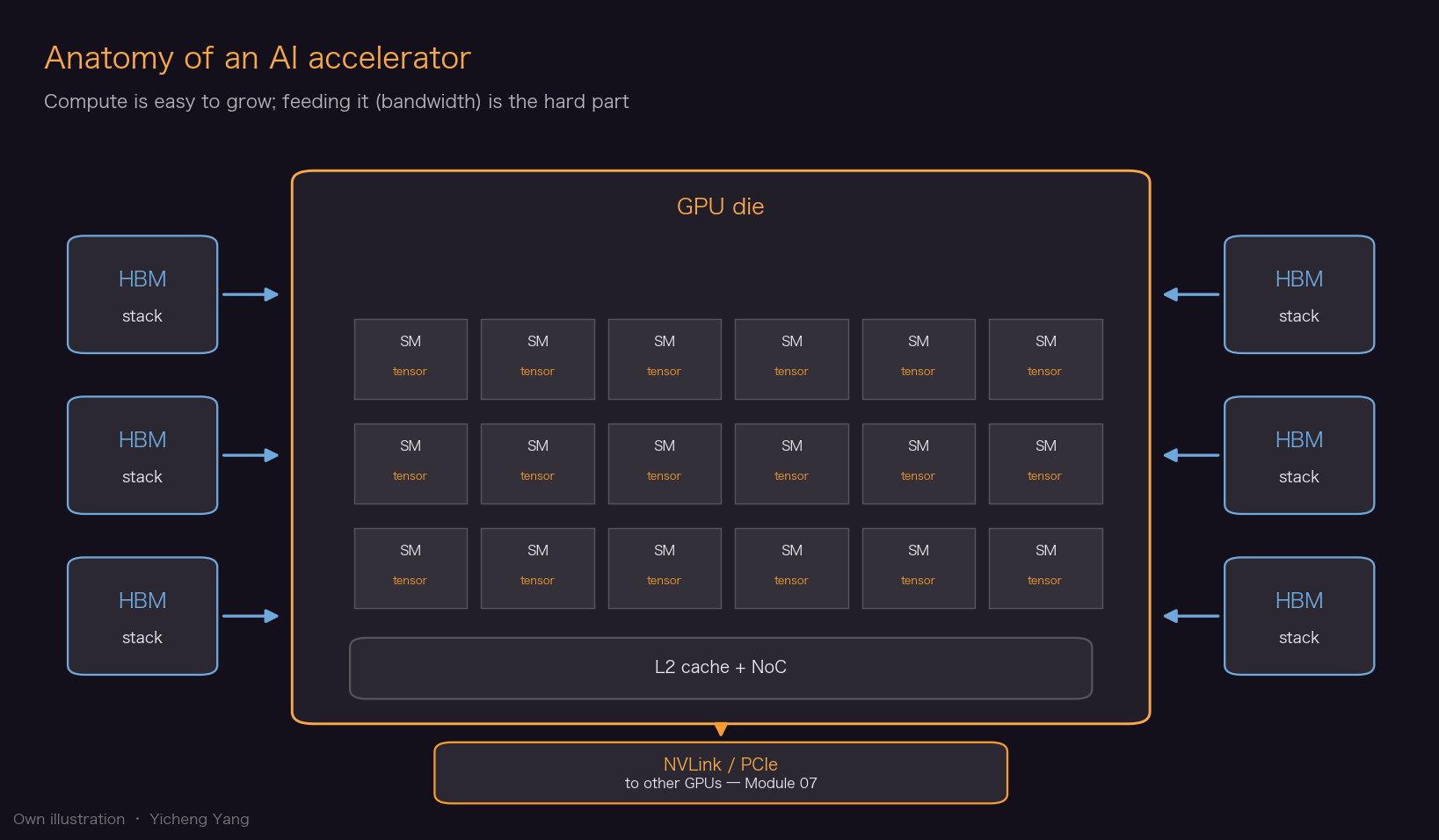
The organizing unit is the Streaming Multiprocessor (SM) — an H100 carries 132 of them. Inside an SM, threads are not scheduled one by one: they are bundled in groups of 32 called warps, and the hardware issues one instruction that all 32 threads execute simultaneously, each on its own piece of data. Nvidia calls this SIMT — single instruction, multiple threads. The point is amortization: fetching and decoding an instruction is expensive, so you do it once and harvest 32 results.
This design fits neural networks almost embarrassingly well. Training and inference consist of applying the same multiply-and-add to millions of numbers, with essentially no branching — exactly the shape of work a SIMT machine devours.
Finally, hold the three-level memory picture: each thread has private registers; threads in a block share a fast scratchpad inside their SM; and everything ultimately loads from the big off-chip memory stack, HBM. The entire economics of AI hardware hangs on how rarely you can afford to touch that outermost level.
Tensor Cores and systolic arrays: engines that do nothing but matrix math
Why did GPUs sprout dedicated matrix hardware? Energy accounting. In a GPU pipeline, issuing an instruction costs roughly 30 picojoules, while the floating-point multiply-add it triggers costs only about 1.5 pJ — a 20x overhead. The paperwork costs twenty times more than the work. The fix is fatter instructions: with Volta (2017), Nvidia introduced the Tensor Core, hardware that executes one fused instruction performing an entire small matrix-multiply-and-accumulate. One instruction issue now buys hundreds of operations, and the overhead is amortized away. Every generation since — Ampere, Hopper, Blackwell — has enlarged the matrix 'tile' each instruction chews through.
Google's TPU pushes the same logic to its endpoint. Its Matrix Multiply Unit is a systolic array: a fixed 256x256 grid of multiply-accumulate cells. Weights are pre-loaded and stay put; input data pulses through the grid in rhythmic waves (hence 'systolic', as in heartbeat), and partial results pass directly between neighboring cells — never visiting a register file, never waiting on an instruction. Control overhead approaches zero. Per SemiAnalysis, Nvidia's effective array went from roughly 32x32 in Hopper to 64x64 in Blackwell, still far below the TPU's 256x256: bigger arrays reuse data better and burn less energy per operation, but are harder to program and fit fewer workload shapes.
That is the whole GPU-versus-ASIC divide in one sentence: the GPU wraps its matrix engines in a flexible SIMT machine that can run anything; the TPU bets nearly the entire die on a single operation, executed with unmatched efficiency.
The real speed limit: arithmetic intensity and the roofline
Every spec sheet leads with FLOPS — floating-point operations per second. But FLOPS only answer 'how fast could the chip compute if the data were already in place.' The other number, memory bandwidth, answers 'how fast can data arrive.' Picture a restaurant kitchen: FLOPS are chefs, bandwidth is the waiters carrying ingredients. Hire a hundred chefs with three waiters and the chefs mostly stand idle.
The bridge between the two is arithmetic intensity: how many operations you perform per byte fetched from memory. The roofline model then compresses everything into one line: attainable performance = min(peak FLOPS, intensity x bandwidth). Plotted, it is a slanted roof that climbs with intensity (bandwidth-limited), then flattens at the compute ceiling.
Plug in an H100 SXM: about 1,979 TFLOPS of dense FP8 compute against 3.35 TB/s of HBM3 bandwidth. You need roughly 590 FP8 operations per byte moved just to keep the arithmetic units busy. Below that threshold you are memory-bound, and buying more FLOPS is money wasted; above it, compute-bound.
Matrix multiplication is the rare workload that can climb the roof: as matrices grow, compute rises with n cubed while data movement rises with n squared, so intensity grows with scale. That is why large-batch training and prompt processing (prefill) run compute-bound. But generating tokens one at a time (decode) re-reads the entire model's weights plus a growing KV cache for every single token while doing trivial math per byte — intensity of order one, hopelessly memory-bound. This one distinction explains why HBM became the industry's chokepoint, and why inference silicon is splitting in two: Nvidia's Rubin CPX piles cheap GDDR7 and raw FLOPS into a dedicated prefill chip, while decode hardware piles on HBM bandwidth.
Shrinking the numbers: FP32 to FP4
A floating-point number is binary scientific notation: one sign bit, exponent bits that set the range, mantissa bits that set the precision. FP32 spends 32 bits per number. Cut the bits and everything improves at once: more multipliers fit in the same silicon area, and more numbers fit through every byte of memory and bandwidth — you raise the compute ceiling and effectively fatten the memory pipe in the same stroke. Each halving of precision roughly doubles throughput.
Neural networks tolerate this surprisingly well because they are statistical systems that absorb noise. So training moved from FP32 to BF16; Hopper introduced FP8; Blackwell introduced FP4. An FP4 number can take only 16 distinct values — used naively, that crushes the data. The trick is microscaling (the MXFP formats, and Nvidia's more accurate NVFP4): numbers are stored in small blocks that share one scaling factor, recovering dynamic range while keeping 4-bit throughput.
The payoff is measured, not theoretical. SemiAnalysis's InferenceX v2 benchmark, run across roughly 1,000 GPUs, shows a GB300 NVL72 delivering up to 100x an H100's inference throughput when the H100 runs FP8 and Blackwell runs FP4 — and 65x when both run FP8. Read the gap between those two numbers carefully: a large share of each 'hardware' generation's gain is really the number format, which only pays off once software and numerical methods mature. The flip side is triage under a fixed silicon budget: to make room for low precision, Nvidia has been shrinking FP64 (scientific-computing precision) support generation by generation.
The accelerator is now a rack
No single chip can hold, let alone serve, a frontier model. Its weights are sharded across dozens to thousands of chips that must exchange partial results after every layer of computation — so the wires between chips became part of the computer, and vendors now compete on scale-up world size: how many accelerators are fused into one high-bandwidth domain that software can treat as a single giant chip.
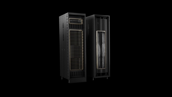
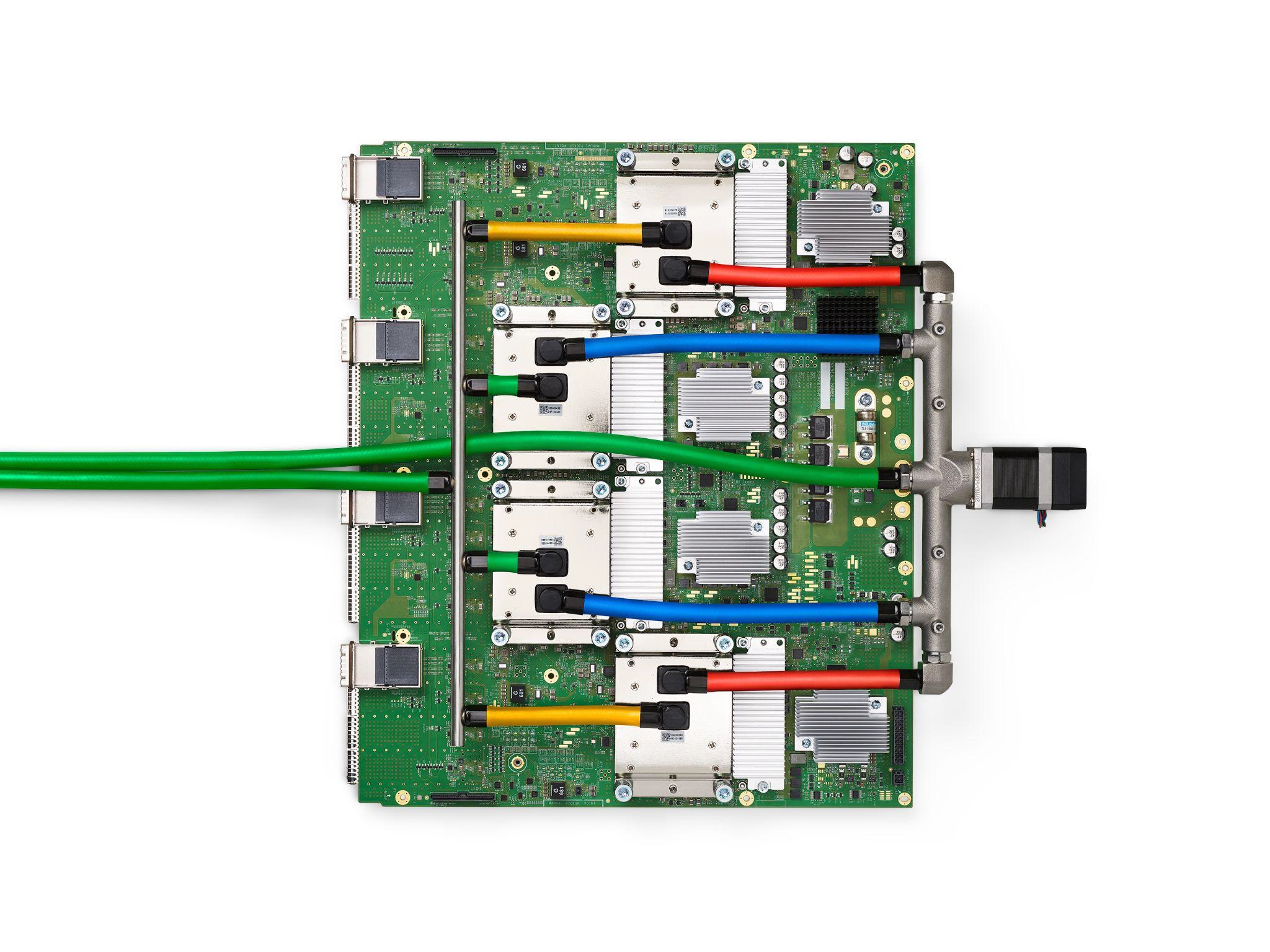
Nvidia's GB200 NVL72 is the emblem of this shift: one liquid-cooled rack holding 72 Blackwell GPUs and 36 Grace CPUs on a single NVLink domain — Nvidia's own press materials describe it as 'acting as a single GPU' with 1.4 exaFLOPS and 30 TB of fast memory. Google answers with the TPUv7 pod: 9,216 chips arranged in a 3D torus and stitched together by 48 optical circuit switches. AMD's MI355X still tops out at 8 — a single number that, per SemiAnalysis, keeps it out of frontier reasoning inference until the MI450X rack arrives.
Two consequences follow. First, TCO replaces price: a GB200 NVL72 costs about 1.6x an H100 cluster all-in, so it must prove itself more than 1.6x faster to be worth buying, and the reliability of a 72-GPU rack is the hidden tax. Second, the system includes software: H100 training efficiency (MFU) climbed from 34% to 54% in BF16 within twelve months with zero hardware change, purely from CUDA library updates — a compounding moat no spec sheet shows. Die plus HBM plus packaging plus fabric plus power plus compiler stack: the sector chapters that follow dissect that full system one layer at a time.

Key Numbers
| Metric | Value | Source |
|---|---|---|
| Energy to issue one GPU instruction vs the FP16 math op it triggers | ~30 pJ vs ~1.5 pJ (20x overhead) — the reason Tensor Cores exist | SemiAnalysis — NVIDIA Tensor Core Evolution: From Volta To Blackwell |
| H100 SXM: peak FP8 compute vs HBM3 bandwidth | 3,958 TFLOPS FP8 (with sparsity) vs 3.35 TB/s; 80 GB HBM3 | NVIDIA — H100 Tensor Core GPU (official specifications) |
| Matrix-engine array size: Nvidia vs Google TPU | Hopper ~32x32 → Blackwell ~64x64; TPU 256x256 | SemiAnalysis — NVIDIA GTC 2025 - Built For Reasoning, Vera Rubin, Kyber, CPO, Dynamo Inference |
| GB200 NVL72 rack contents ('acts as a single GPU') | 72 Blackwell GPUs + 36 Grace CPUs, one NVLink domain; 1.4 exaFLOPS, 30 TB fast memory | NVIDIA Newsroom — NVIDIA Blackwell Platform Arrives to Power a New Era of Computing |
| TPUv7 Ironwood maximum scale-up pod | 9,216 TPUs in one 3D-torus domain, via 48 optical circuit switches | SemiAnalysis — TPUv7: Google Takes a Swing at the King |
| H100 training-efficiency (MFU) gain from software alone, 12 months | BF16 MFU 34% → 54% (+~59% throughput), zero hardware change | SemiAnalysis — H100 vs GB200 NVL72 Training Benchmarks: Power, TCO, and Reliability Analysis, Software Improvement Over Time |
| GB300 NVL72 vs H100 inference throughput (format included) | up to 100x (H100 FP8 → GB300 FP4); 65x if both run FP8 | SemiAnalysis — InferenceX v2: NVIDIA Blackwell Vs AMD vs Hopper |
Sources
- SemiAnalysis — NVIDIA Tensor Core Evolution: From Volta To Blackwell
- NVIDIA — H100 Tensor Core GPU (official specifications)
- SemiAnalysis — NVIDIA GTC 2025 - Built For Reasoning, Vera Rubin, Kyber, CPO, Dynamo Inference
- NVIDIA Newsroom — NVIDIA Blackwell Platform Arrives to Power a New Era of Computing
- SemiAnalysis — TPUv7: Google Takes a Swing at the King
- SemiAnalysis — H100 vs GB200 NVL72 Training Benchmarks: Power, TCO, and Reliability Analysis, Software Improvement Over Time
- SemiAnalysis — InferenceX v2: NVIDIA Blackwell Vs AMD vs Hopper
- Wikimedia Commons (CC BY 4.0; Jouppi et al., Google TPUv4 paper)
- Wikipedia — Hopper (microarchitecture), H100 SXM5 specs
- Wikipedia — Single instruction, multiple threads ('warp' composed of 32 hardware threads executed in lock-step)
- Google Cloud — TPU system architecture documentation
- SemiAnalysis — Another Giant Leap: The Rubin CPX Specialized Accelerator & Rack
Related sector deep-dives
Optional — jump ahead if this module is all you needed; otherwise continue the ladder above.